Deep RIE: What is Deep Reactive Ion Etching (DRIE)?

Learn the following in this post
- What is Deep Reactive Ion Etching?
- What is the importance of aspect ratio (depth vs. width of the hole)?
- Are there limits regarding aspect ratio? For instance, is 50:1 a fundamental boundary?
- What expertise does Atomica bring to Deep RIE?
- Has Atomica successfully applied DRIE to particularly exacting specifications?
- Is mastery of Deep RIE critical for bridging the gap between prototyping and high-volume manufacturing?
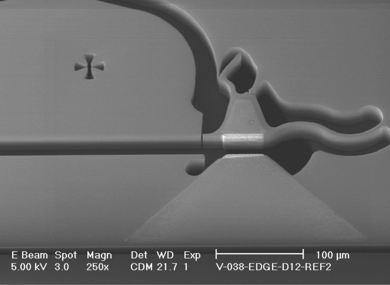
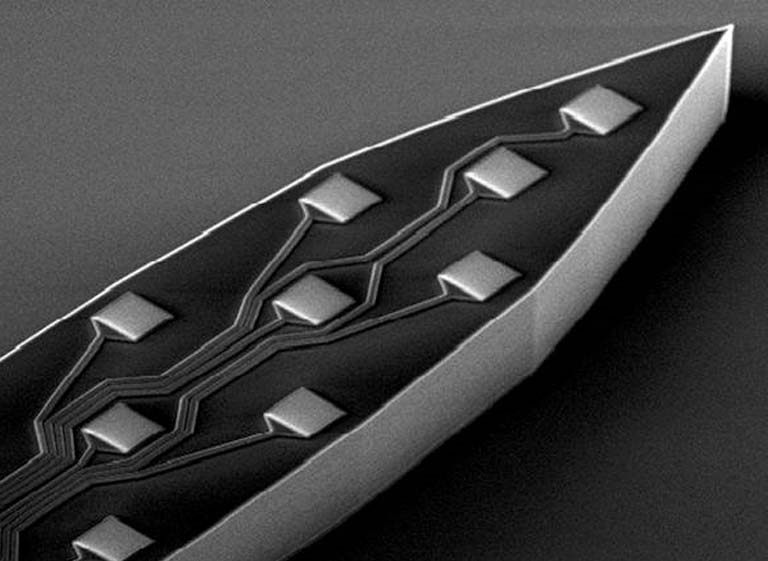
Microelectromechanical systems (MEMS) rely on the etching of very small features into substrates such as silicon. Deep reactive ion etching (DRIE, or Deep RIE) is a plasma-based etching process that yields deep holes and trenches with steep sides. With DRIE, a silicon wafer can be etched anisotropically with high precision, enabling reliable manufacturing of sophisticated MEMS devices. In Fall 2020, Atomica acquired an Omega Rapier plasma etch system that is the state of the art in MEMS etching.
We sat down with several members of the Atomica team to discuss how DRIE and the Rapier system are critical to MEMS. Eric Sigler is the CEO of Atomica, Dr. Brian Maertz is Atomica’s CTO, Dr. Stuart Hutchinson is our Director of Field Applications Engineering, and Theodore Chi is our Director of Global Sales. This interview has been condensed and edited for clarity.
What is Deep Reactive Ion Etching?
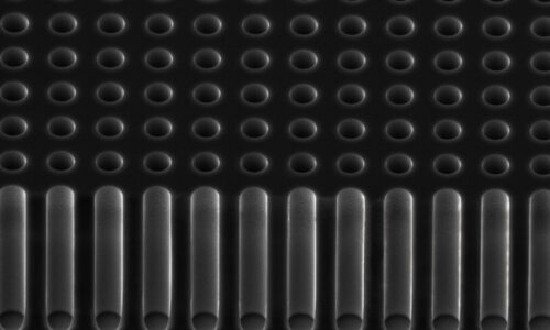
Stuart Hutchinson [SH]: In MEMS, you need to be able to micro-machine (or make holes into) wafers of material, mainly silicon. With DRIE, two different types of plasma are alternating as we make our way down the hole. We have an etch plasma running that etches down and sideways at the same time. To prevent the sideways motion, we stop the etch and light up a different plasma which coats the sidewalls with polymer to protect them. Then we light up the etch plasma again and go down a little bit more, and then we stop it and we light up the polymer coating again. The actual etch cycle is isotropic; the polymer deposition cycle prevents it being isotropic all the way through, to keep the etch in a vertical direction. This is known as the Bosch process.
Brian Maertz [BM]: You can use it to make very diverse structures, such as one where you’re removing a lot of the wafer and leaving just a little bit behind.
What is the importance of aspect ratio (depth vs. width of the hole)?
SH: High aspect ratio enables things to be closer together.
Eric Sigler [ES]: And that’s important. Our ability to provide more value to our customers in terms of resolution and density is a function of the aspect ratio. Picture a gyroscope or things with a comb drive, where you’re interdigitating fingers. Or maybe you’re making microinductors and there needs to be separation between the insulator and the material. There are many mechanical objectives that we’re trying to hit for our customers that depend on achieving very fine features.
BM: …and creating them the same every time.
ES: The big push is to get finer and finer accuracy. Consider a gyroscope; fitting more sensory “fingers” into this thing would give you finer resolution. You can measure capacitance of the gyroscope better, which helps you know if it’s tilting with more precision. An iPhone is just trying to tell if you’ve flipped the thing up or down, whereas a MEMS-enabled car is trying to determine—in the middle of a city where you can’t get a GPS signal—did I just take a right turn of 20° or 40°? And how far have I traveled since I last had my GPS connection? And that’s going to tell you where you are on the map, which might indicate if you’re about to hit a building versus staying on the road. Finer and finer precision is critical for other applications like missiles that are being guided to hit an incoming weapon. In all these cases, you need to know exactly where you are.
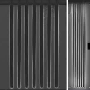
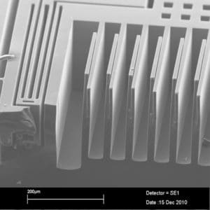
SH: The aspect ratio argument also lends itself to the miniaturization argument as well. You can pack more of these interdigitated fingers into a smaller space because you can etch narrower gaps down between them.
BM: And for that, we have a Rapier that achieves the highest aspect ratio of any DRIE tool.
Are there limits regarding aspect ratio? For instance, is 50:1 a fundamental boundary?
ES: I believe roughly 50:1 is a practical limit today for large or deep etches.
SH: There are some physical limits involved, but vendors are continually developing their systems to circumvent or mitigate those physical limits.
BM: It’s all about factors such as the switching speeds of valves and stuff like that so that you can switch between the etch and the passivation very quickly.
ES: Tilt control also becomes paramount for many of these structures.
BM: Yes, tilt control is a lot of what allows you to do very high aspect ratios—making sure that the sidewall angle is exactly 90°. We can pattern the wafer from one side and then pattern it on the other side as well. Ensuring that things are very well aligned from one side to the other
enables you to do things that you couldn’t do otherwise.
What expertise does Atomica bring to Deep RIE?
BM: We’ve successfully achieved the specifications of many different state-of-the-art devices. Whatever the next thing is, we’ve seen that before, so we know how we would approach most problems.
SH: There are many people in the company that understand DRIE, to a pretty deep level. It’s our vast collective experience.
ES: Yes, it’s the breadth of our team and the number of people that have expertise. It’s the number of different situations, scenarios, and structures we’ve seen. It’s the number of problems that we’ve encountered and overcome.
Theodore Chi [TC]: It’s important to note that DRIE can also be used for die singulation. And it’s particularly useful for very precise, odd-shaped, pre-rounded die – something that cannot always be accomplished with transitional dicing saws or stealth methods.
Has Atomica successfully applied DRIE to particularly exacting specifications?
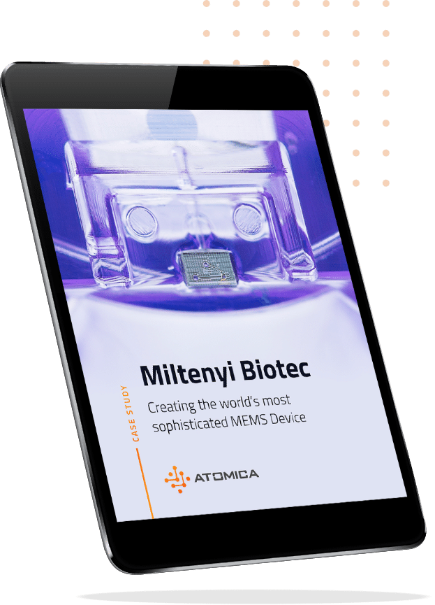
BM: Regularly. [laughs] One example is the Miltenyi Biotec cell sorter that we manufacture and helped design. It’s very critical that we get a specific gap control. The passageway is as narrow as possible and has to be very vertical. The specification is very tight and we do that etch regularly. There are other portions of the wafer where we’re etching a very large area and we have to get the etching to work in both areas (deep and shallow) at the same time. That’s particularly challenging.
Is mastery of Deep RIE critical for bridging the gap between prototyping and high-volume manufacturing?
BM: Definitely! It’s not just figuring out how to make something once, it’s making sure you have a process robust enough to repeat. We understand that from the beginning.
ES: It’s easy to test an electrical circuit to see if it works right—run an algorithm to see if it did what you expected. When you’re testing a mechanical structure like a deep feature that’s been etched, we often have to take these things out and go put them in the scanning electron microscope. Or maybe we have to dice the wafer and destroy it in order to see if it has the structure that we’re going after. If you don’t have a consistent, repeatable, well dialed-in process, you can’t achieve good yield or move a program to volume production.
BM: Variation is inherent in etch processes because you have variation in the condition of the chamber and in the incoming material. Plus standard tool variation. So being able to know, definitively, when you’re done etching is critical.
ES: It’s really important to know when to stop etching because you don’t want to go too far or you’ll destroy your structure, and you don’t want to go too shallow or you won’t get the device performance that you were going for.
BM: Endpoint detection is critical and the Rapier has very sensitive endpoint detection. Essentially what it’s doing is measuring the chemistry of the byproduct of the etch. That, combined with the very good uniformity that we get across wafer, allows you to stop right where you want to.
ES: Brian mentioned uniformity; as you move out on the wafer or as you’re etching more and more of the wafer, the notion of fill factor is relevant. If you’re making one little hole on a die and it’s tiny and it’s only covering 1% of the wafer, that’s relatively easy to do and it’s quick. But if you’re trying to etch a thousand holes on the device and those holes represent 70% of the silicon area, you now have a more challenging etch to make. And similarly, as you go into 8” wafers, you want those holes out on the periphery of the wafer to be the same as the holes at the center of the wafer. And that’s where having both process control and the most advanced tool in the industry are important.
What cost benefits are associated with a state-of-the-art Deep RIE tool like the Rapier?
ES: The ability to etch quickly changes the economics. These are multi million dollar tools. This contributes significantly to the cost of the product. Having a tool that can etch quickly means you don’t have to utilize the tool as long, which means we can make a device cheaper than someone else who has an older DRIE tool. I think it’s accurate to say that we have the most advanced DRIE of any MEMS foundry and Atomica is perhaps the only pure-play MEMS foundry in the world with an 8″ Rapier capability.
To sum up, why should someone choose Atomica as their MEMS development and manufacturing partner?
BM: Because whatever you want us to do, we’ve already seen it. Somewhere between 70% and 80% of our programs are dependent on DRIE.
TC: Brian took the answer right out of my mouth! We’ve done so many different MEMS programs that we know—before the customer even knows where they want to end up—how to take them there.
SH: World-class expertise. World-class technology.
ES: DRIE is core to what we do. You generally can’t make a MEMS device unless you’re good at DRIE. This isn’t part of our competitors’ bread and butter; for example, CMOS fabs generally don’t need to make these kinds of structures.
At Atomica, we’re striving to unleash the power of microelectromechanical systems (MEMS) with clients that are solving the great problems of our time. Our MEMS production fab—the largest pure-play MEMS foundry in the USA—with a variety of cutting-edge tools and capabilities aligned to get our customers into production.