MEMS Foundry
Atomica is the largest MEMS foundry in the US, providing close collaboration in particular for North American customers and the assurance that intellectual property is protected and respected. The company is privately held and controlled by Cerium Technology.
Atomica has been operating for over 20 years. Our MEMS Foundry recently underwent a two-year transformation with improved systems and an 8” (200mm) wafer line. The recent purchase of more than 300 state-of-the-art semiconductor processing tools has marked a key milestone in our MEMS Foundry transformation. It has expanded Atomica’s capability to develop and manufacture sophisticated microdevices, biochips and sensors.
MEMS Foundry Details
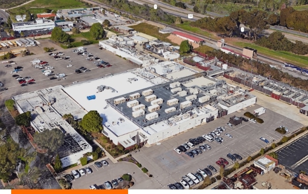
- 13-acre, 130,000 ft2 manufacturing facility with the capacity to support high volume production
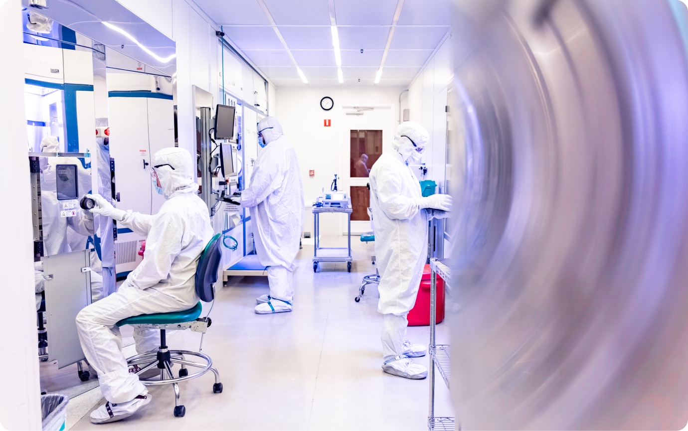
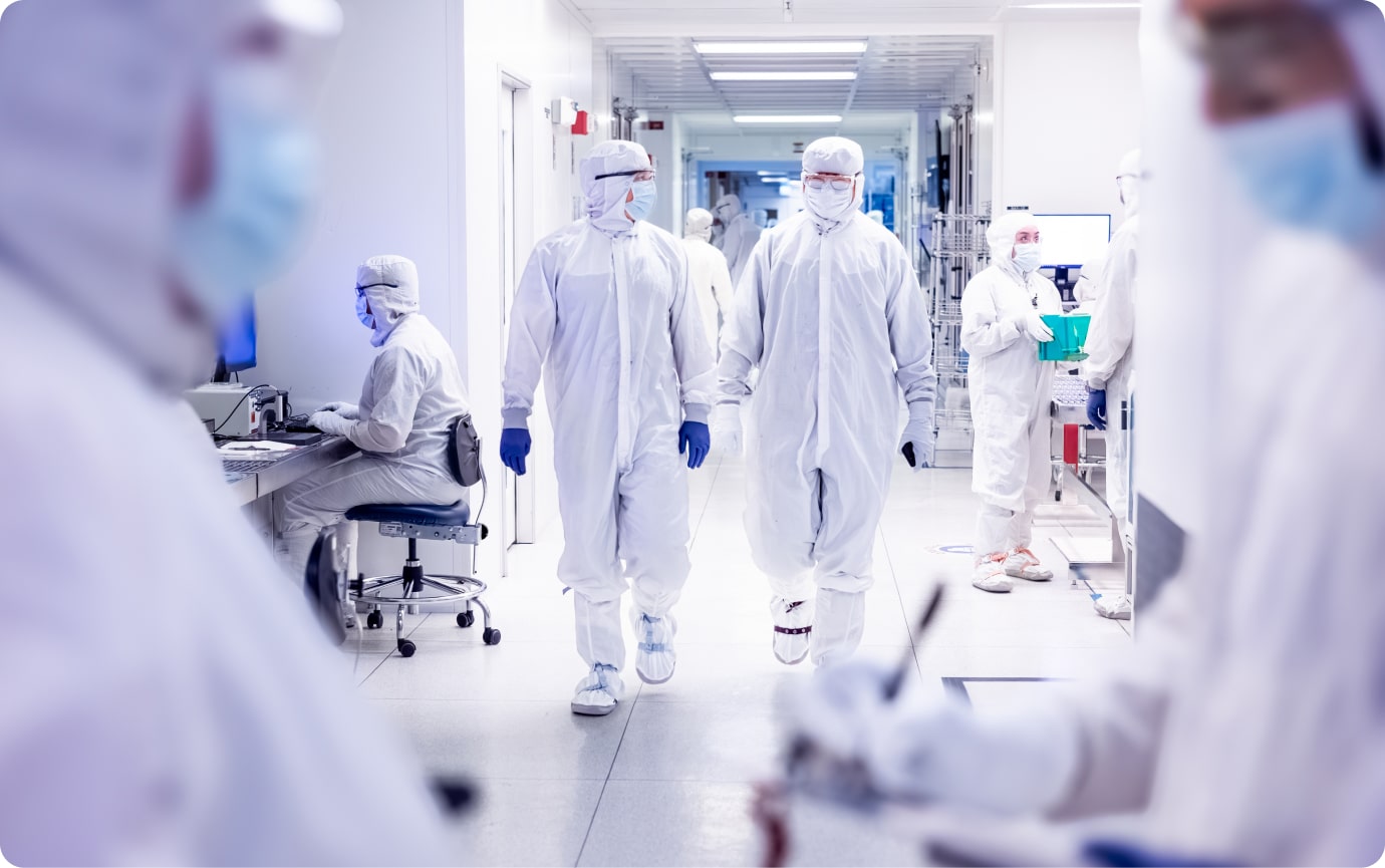
- 30,000 ft2 class 100 cleanroom
- Over 400 tools for both 6” and 8” wafer production
- ISO 9001 certified (since 2006)
- ISO 13485: 2018 compliance in progress (Medical Quality System Regulation)
- IATF 16949: 2016 compliance in progress
- Mature MES, document control, and phase-gate systems
- ITAR registered
- Broad materials flexibility, providing access to an extensive set of processes and materials unavailable in CMOS fabs, including noble metals, polymers, and virtually any substrate (e.g., silicon, SOI, glass, fused silica, quartz, borosilicate, piezos, and III-V).
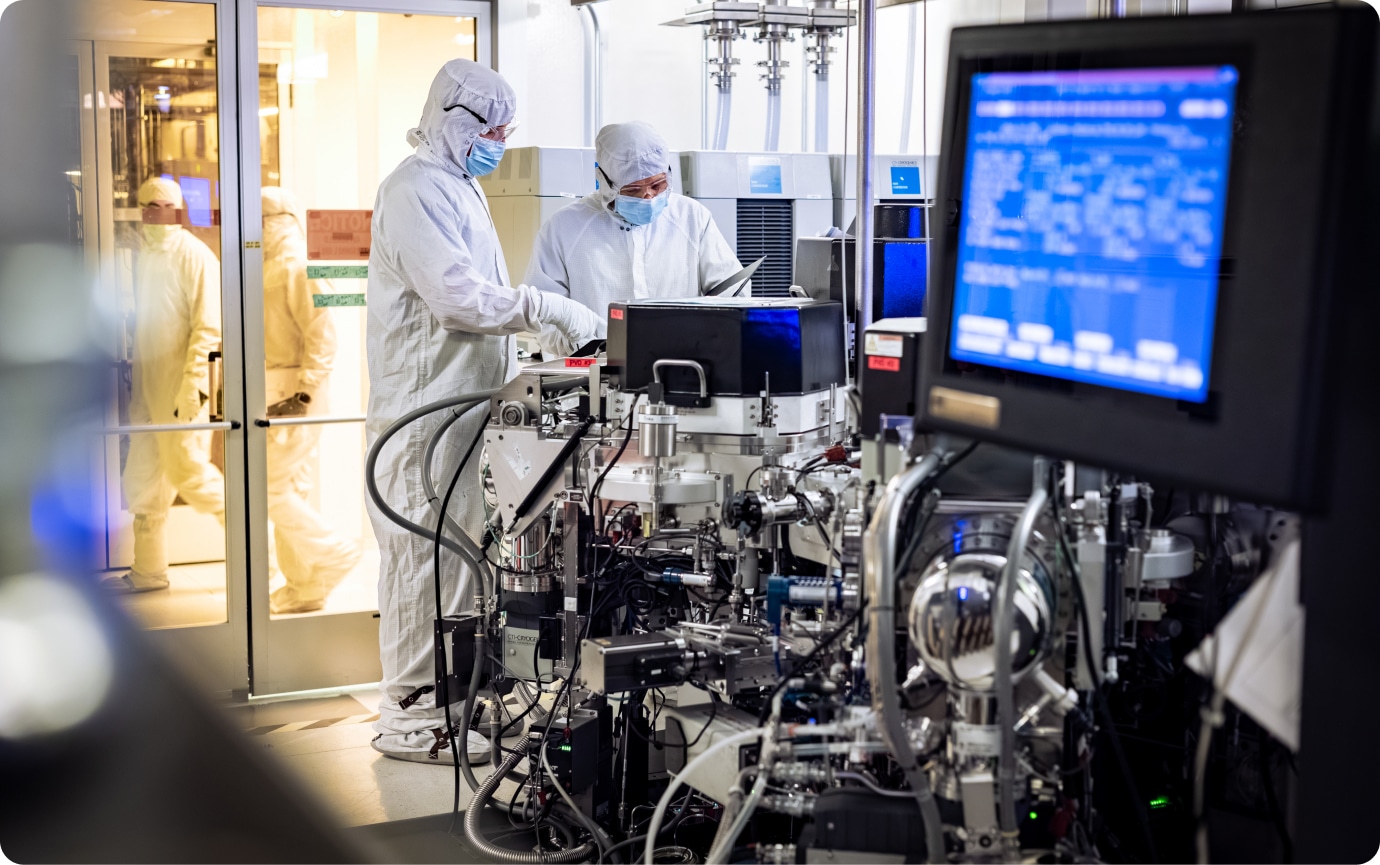
New 200 mm-compatible equipment include:
- Applied Materials Endura PVD for precise sputtered films
- Veeco Phoenix atomic-layer deposition (ALD) system enabling atomic-scale high quality conformal coatings
- Evatek Evaporator for high-volume deposition of evaporated films and optical coatings
- Plasma-Therm High Density PECVD for high quality lower-temperature dielectric films with superior gap fill
- Plasma-Therm RIE etch cluster for a variety of production uses
- Multiple production-grade lithography systems from Suss and OAI
- Over 100 new advanced metrology systems including automated optical inspection
- Nearly a dozen new automated wet benches.
MEMS Foundry in Santa Barbara
We are located in the Santa Barbara area (Goleta, California) next door to the University of California, Santa Barbara, one of the top engineering universities in the world. This talent pool combines with Atomica’s multi-disciplinary team of scientists and manufacturing engineers to tackle the hardest process development and integration challenges with an eye toward manufacturability (DFM).


Why Atomica?
At Atomica, we prioritize the success of our customers’ products through rapid prototyping and scalable production. As a leader in microfabrication for photonics, sensors, biotechnology, and MEMS, we offer device optimization, faster time to market, and cost-efficient fabrication. Our 30,000-square-foot class 100 cleanroom near Santa Barbara, California, holds ISO 9001 certification and ITAR registration, ensuring the highest standards of quality and regulatory compliance. With advanced process control analytics, AI-driven inspection, cutting-edge metrology, and proprietary fab operations systems, we maximize efficiency and product reliability.
Atomica’s ability to deliver rapid prototyping and scalable production is built on five key differentiators: