Bonding Technologies
Atomica works closely with the customers’ needs to determine the appropriate bonding method. Frequently, multiple bonding methods can be combined to achieve the desired final packaging. In addition to hermeticity requirements, other considerations include:
- Design/device footprint
- Temperature budget
- Materials used
- Final packaging and environmental requirements
Atomica Bonding Capabilities:
- Anodic Bonding Anodic bonding is a technique that creates a permanent bond between a silicon wafer and a glass substrate. This process involves applying a voltage across the interface while heating the materials to 300–450°C, causing the sodium ions in the glass to migrate and form a strong electrostatic bond.
- Fusion Bonding (Direct Wafer Bonding) Fusion bonding, also known as direct wafer bonding, is a process in which two smooth, clean, and flat wafers are pressed together at room temperature, creating a bond through atomic interaction. Subsequent thermal annealing enhances the bond strength.
- Thermocompression Bonding Thermocompression bonding is a process in which two materials are bonded under heat and pressure, creating a solid-state bond. Metals such as gold or copper are typically used due to their ability to form strong bonds at lower temperatures.
- Eutectic Bonding Eutectic bonding occurs when two materials are bonded together at a temperature lower than their individual melting points, forming an alloy at the interface. This bonding is typically performed between metals like gold and silicon, or gold and tin.
- Polymer Bonding Polymer bonding uses polymeric materials, such as adhesives or resins, to bond two substrates together. This can be done by applying heat or pressure to cure the polymer and create a bond.
- Metal Bonding Metal bonding involves joining two metal surfaces through techniques like soldering, diffusion, or thermocompression, often using materials such as gold, copper, or solder alloys.
- Frit Glass Bonding Frit glass bonding uses a low-melting-point glass frit to bond wafers or components together. The glass frit is deposited onto one substrate and heated to a temperature where it softens and bonds with another substrate.
- Mounting with Polymer Temporary mounting with polymer involves bonding a wafer or device to a handling substrate using a polymer adhesive, which can be removed later without damaging the wafer.
- Demounting Demounting involves the careful removal of a bonded wafer from its temporary substrate, often achieved by dissolving or peeling away the adhesive used during temporary mounting.
- Tape/Dry Film Based Bonding/Mounting Tape or dry film bonding uses adhesive tapes or dry films to bond two wafers or a wafer to a carrier temporarily. These films can often be removed without residue.
For more details on our bonding capabilities, please contact our technical team or download our fab technology guide.
Other Capabilities
Why Atomica?
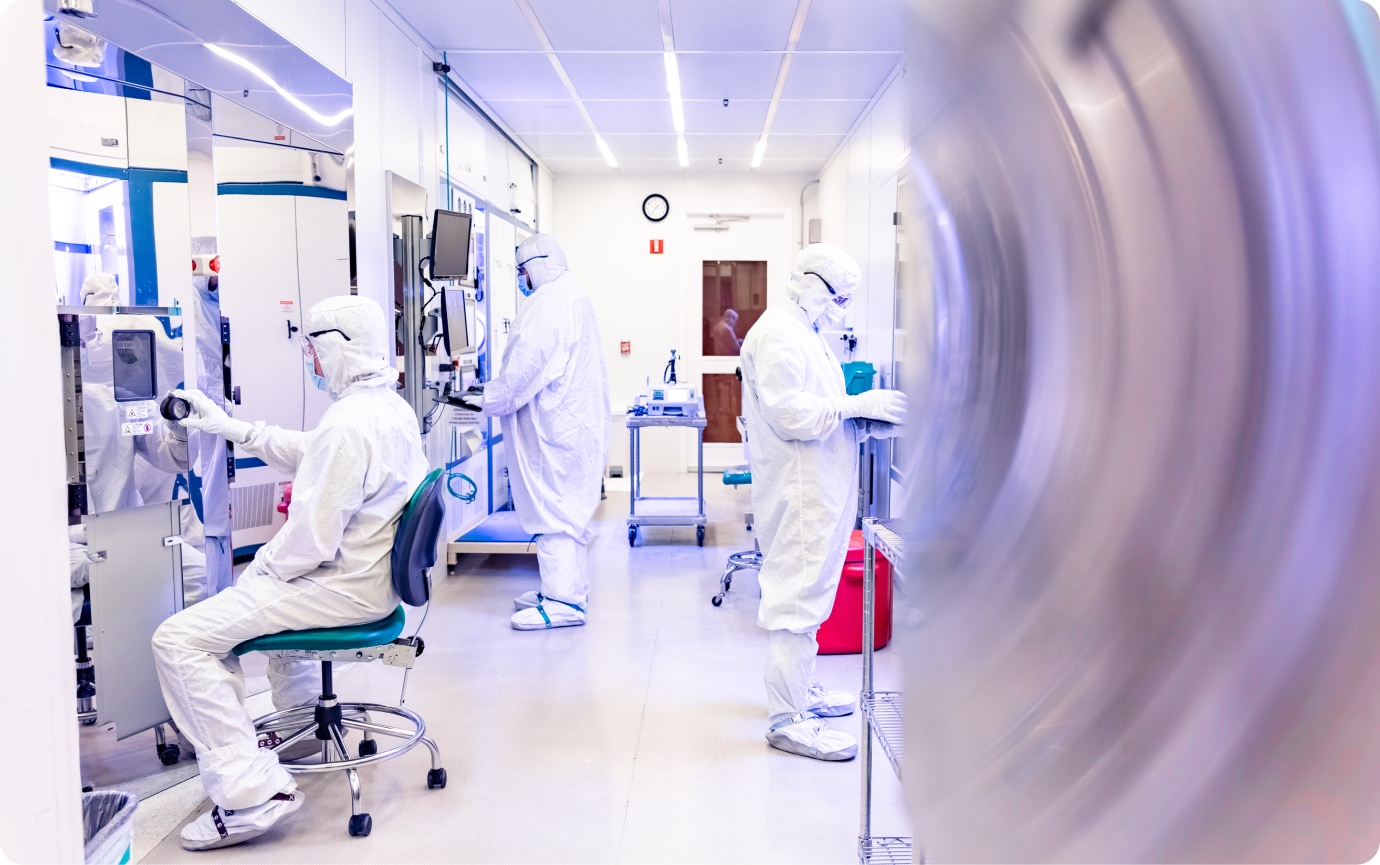
Atomica focuses on the success of our customers’ products, with rapid prototyping and scalable production. We are a leader in microfabrication, including photonics, sensors, biotechnology, and MEMS. We provide customers device optimization, faster speed to market, and cost-efficient fabrication. Atomica operates a 30,000-square-foot class 100 cleanroom near Santa Barbara, California, supporting a wide range of capabilities and materials with ISO 9001 certification and ITAR registration. We leverage sophisticated process control analytics, artificial intelligence inspection, advanced metrology, and proprietary fab operations systems to maximize efficiency.


Next Steps

Learn Wafer Bonding Techniques and its importance for MEMS

Talk to our engineering team about your Wafer Bonding needs

Download our comprehensive eBook on Wafer Level Packaging