
Atomica’s Deposition Capabilities
Atomica has a whole host of different targets under vacuum in multiple production-class cluster tools, from RF and DC magnetron systems to evaporators, LPCVD, and PECVD. We offer the following capabilities:
- Physical Vapor Deposition (PVD) PVD is a vacuum-based deposition method where material is vaporized from a solid source and deposited as a thin film onto a substrate. Common PVD techniques include sputtering and evaporation, where material is either ejected by ion bombardment or vaporized through heating.
- Chemical Vapor Deposition (CVD) CVD involves the chemical reaction of gaseous precursors that decompose on a heated substrate, forming a solid material. It allows precise control over film composition and thickness.
- Plasma Enhanced Chemical Vapor Deposition PECVD enhances the traditional CVD process by using plasma to activate chemical reactions at lower temperatures, allowing for deposition on temperature-sensitive substrates.
- Low Pressure Chemical Vapor Deposition (LPCVD) LPCVD is a variant of CVD performed under low pressure, promoting uniform film deposition over large surface areas. It offers excellent step coverage and is often used in high-temperature processes.
- High Plasma Density CVD (HDPCVD) HDPCVD uses a high-density plasma to enhance the deposition process, allowing for excellent gap-filling and conformal coverage, particularly useful in high-aspect-ratio structures.
- Atomic Layer Deposition (ALD) ALD is a precise thin-film deposition technique where films are grown one atomic layer at a time. It alternates between two precursor gases, each reacting with the substrate to form a monolayer, allowing for atomic-scale thickness control.
- Ion beam deposition (IBD) IBD uses an ion beam to sputter material from a target, which is then deposited onto a substrate. The ion beam can also be used to modify film properties or clean the substrate prior to deposition.
- E-Beam Evaporation E-beam evaporation is a physical vapor deposition technique where an electron beam is used to heat and vaporize material in a vacuum. The vaporized material then condenses onto a substrate to form a thin film.
- Thermal Oxidation Thermal oxidation is the process of forming silicon dioxide (SiO2) by exposing silicon wafers to oxygen or steam at high temperatures. This oxidation process creates a high-quality insulating layer on the silicon surface.
For more details on our deposition capabilities, please contact our technical team or download our fab technology guide.
Other Capabilities

Why Atomica?
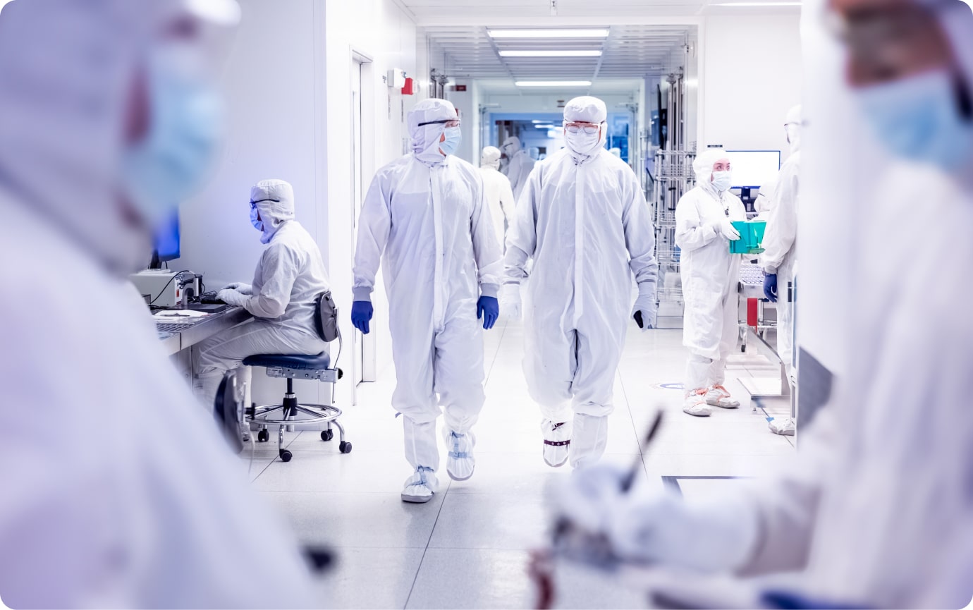
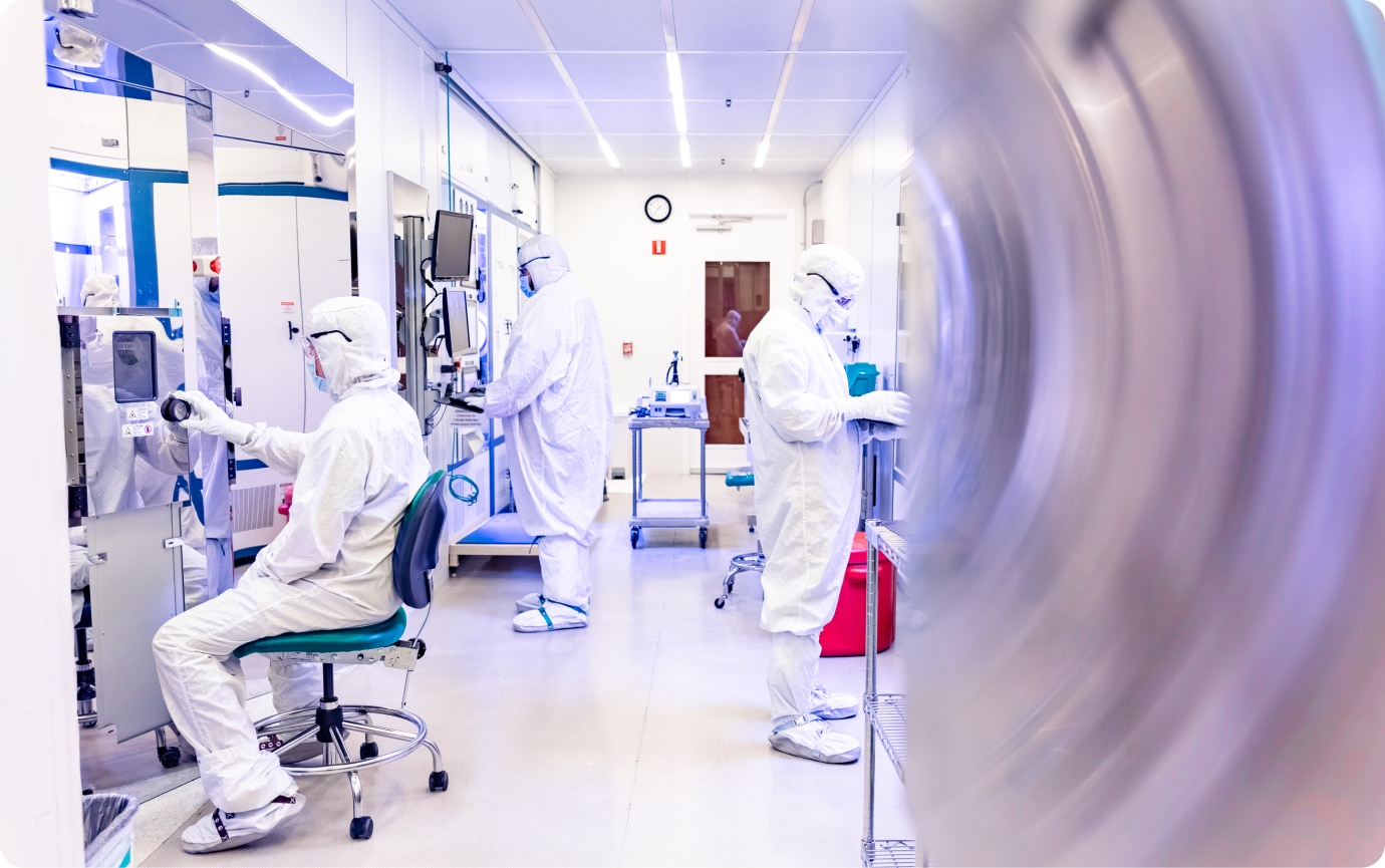
Atomica focuses on the success of our customers’ products, with rapid prototyping and scalable production. We are a leader in microfabrication, including photonics, sensors, biotechnology, and MEMS. We provide customers device optimization, faster speed to market, and cost-efficient fabrication. Atomica operates a 30,000-square-foot class 100 cleanroom near Santa Barbara, California, supporting a wide range of capabilities and materials with ISO 9001 certification and ITAR registration. We leverage sophisticated process control analytics, artificial intelligence inspection, advanced metrology, and proprietary fab operations systems to maximize efficiency.
Next Steps
Download our comprehensive eBook on Wafer Level Packaging
Talk to our engineering team about your deposition project
Read about our investment in cutting-edge MEMS tools