Atomica is a U.S.-based microfabrication foundry offering platforms for AI infrastructure, photonics, sensors, biotechnology, and MEMS. Through rapid prototyping, scalable production and deep process-integration expertise, Atomica helps customers develop and manufacture the precision structures behind AI hardware, optical communications, healthcare, aerospace and defense, industrial, automotive, and consumer products.
AI Infrastructure
Discover how Atomica makes AI hardware manufacturable: the enabling structures for optical connectivity, photonic integration, thermal management, and physical AI sensing, from prototype to volume.
Photonics
Discover Atomica’s photonics technologies which empower optical communications, 3D sensing and LiDAR, augmented/virtual reality (AR/VR), thermal imaging, illumination, and other types of optical sensing.
Sensors
Atomica makes MEMS for thermal imaging, inertial measurement, microphones, gas and chemical detection, biological sensing, magnetics, pressure sensors and more.
Biotechnology
From drug-delivery devices to neural probes, cell sorters to biosensors, DNA synthesis to sequencing, learn how Atomica’s capabilities bring your biotechnologies to life.
MEMS
Atomica has worked on hundreds of different MEMS projects. We have the capability and experience to support the custom design and production of virtually any type of MEMS device.
Other Microfabrication?
Tell us what you’re building and we’ll map it to the right platform. Talk to an Atomica engineer about your device, materials, and path to production.
Explore Atomica’s in-depth resources to navigate modeling and simulation, rapid prototyping, scalable production, and fab evaluation — all with expert insight.
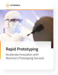
Rapid Prototyping Services at Atomica
Uncover our efficient process that turns ideas into working prototypes swiftly, helping you bring innovations to life quickly.
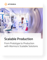
Scaling Production with Atomica’s Expertise
Explore how our advanced production methods ensure consistent, high-quality, and cost-effective results at every stage of scale.

Inside Atomica’s Advanced Fab Technology
Take a detailed look at our high-tech capabilities, engineered to support complex, precision-driven microfabrication.

Selecting the Right Fab for Your Project
Our Fab Evaluation Guide outlines essential criteria, ensuring your project is matched to the best fabrication partner.
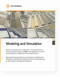
Simulation-Driven Microfabrication
See how modeling and simulation improve performance, lower cost, shorten timelines, and drive better outcomes.
Capabilities
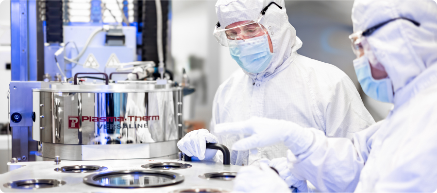
Atomica is dedicated to the success of our customers’ products, offering the fastest and most cost-efficient path to achieving development goals through Rapid Prototyping and Scalable Production. With state-of-the-art equipment, infrastructure, analytics, certifications, and quality assurance, we accelerate time to market while ensuring product excellence. While many fabs provide a range of tools and capabilities, Atomica stands out with its proven expertise in integrating complex layers and diverse materials, understanding their interactions, and delivering seamless, high-performance solutions. This experience is the key to helping our customers succeed in even the most demanding applications.

Design
Read about Atomica’s design and modeling services that complement our wafer foundry capabilities.

Lithography
Learn about Atomica’s photolithography technologies and leading-edge greyscale (3D) lithography.

Deposition
Discover Atomica’s deposition tools and its wide range of metals and dielectric deposition capabilities.

Plating
Discover how Atomica’s extensive range of plating tools and expertise unlock our unmatched material toolbox.

Annealing and Oxidation
Learn how Atomica’s Thermal Oxidation and Annealing processes play a crucial role in enhancing performance.

Dry Etching
Explore Atomica’s Deep Reactive Ion Etching (DRIE), Reactive Ion Etching and various other dry etch capabilities.


Wafer Bonding
Learn how Atomica’s bonding allows hermetic and vacuum wafer-level packaging.

Wafer Backend
Explore Atomica’s backend capabilities from CMP to wafer thinning to dicing.

Wafer Testing
Learn how Atomica’s in-process electrical, mechanical, and thermal testing enables real-time verification of functionality.

Metrology
Read how Atomica’s diverse metrology tools, enhanced with AI analysis, deliver precise, data-driven insights.
Why Atomica?
Atomica’s ability to deliver rapid prototyping and scalable production is built on five key differentiators. Together, they help reduce development risk, improve execution, and create a more direct path from early concepts to manufacturable products.
A manufacturable path from prototype to production
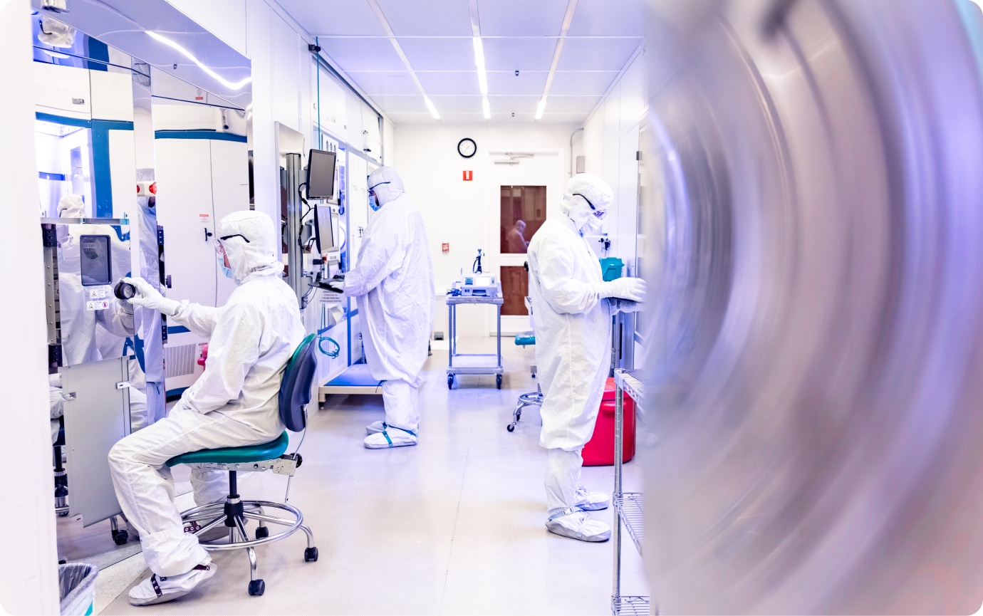
Choose Atomica for the engineering expertise, fab technology, and scalable manufacturing needed to move advanced hardware from prototype to production.
Latest insights
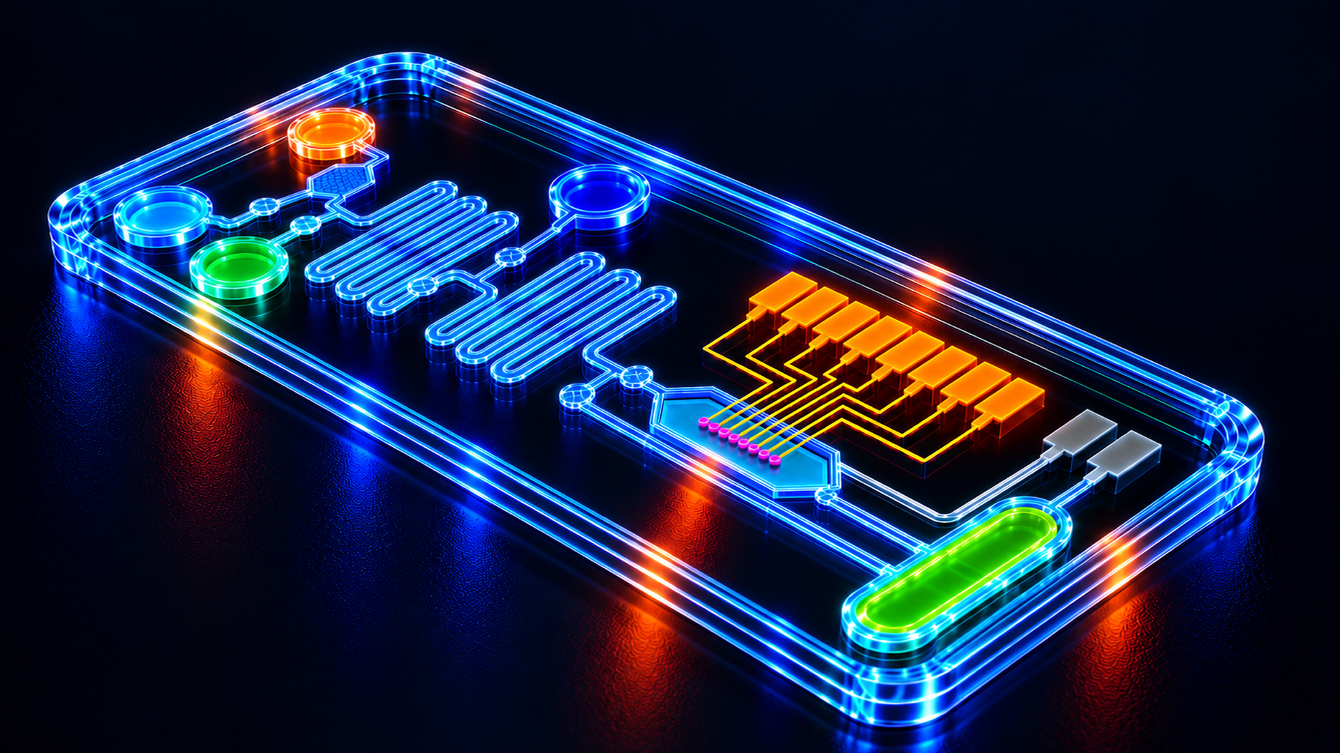
- Atomica Launches Biotechnology Microdevices Platform for Diagnostics and Drug Delivery - Atomica announces its Physical AI Sensor Platform — MEMS, optical, microfluidic and… Read More
- Atomica Launches MEMS Optical Control Platform for Next Generation of Optical and Sensing Systems - Atomica announces its Physical AI Sensor Platform — MEMS, optical, microfluidic and… Read More
- Atomica Launches Physical AI Sensor Platform to Meet a New Wave of Sensor Demand - Atomica announces its Physical AI Sensor Platform — MEMS, optical, microfluidic and… Read More