What is wafer bonding and how does it apply to MEMS?

Learn the following in this post
- What is wafer bonding and how does it apply to MEMS?
- Where does wafer level packaging (WLP) enter this story?
- What is the importance of bond line width?
- Which types of bonds are used most often at Atomica?
- What factors affect the choice of bond?
- What does Atomica bring to the table regarding wafer bonding?
Wafer bonding plays an integral part in microelectromechanical systems (MEMS). To help understand wafer bonding and its role in the electronics industry, we sat down with several members of the Atomica team to discuss: Eric Sigler is the CEO of Atomica, Dr. Brian Maertz is Atomica’s CTO, Dr. Stuart Hutchinson is our Director of Field Applications Engineering, and Theodore Chi is our Director of Global Sales. (Note: this interview has been condensed and edited for clarity.)
What is wafer bonding and how does it apply to MEMS?
Ted Chi [TC]: Wafer bonding is literally sticking two different pieces of material together at the wafer level using different techniques. The two wafers might be separated by an insulator like silicon dioxide, or one of the wafers may have a cavity and the other wafer has some structure that you want to protect under atmosphere or vacuum by bonding the wafers together.
Semiconductor devices are solid-state devices. They’re all electronic circuits. There are no moving parts; There is no requirement for packaging per se. MEMS can be composed of active moving devices. Consider a MEMS relay – a one millimeter by one millimeter device with a switch structure that moves up and down. If it is open to the environment, any kind of particle could get in and that will make the device useless after maybe a few days. When you protect that structure hermetically, then the reliability of the device will last 20 years, for example. In other applications, the actual device doesn’t function or perform unless it’s in an environment like a vacuum.
Where does wafer level packaging (WLP) enter this story?
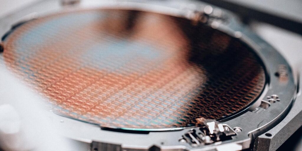
Brian Maertz [BM]: There are two ways to achieve that hermetic packaging or vacuum packaging. One is to do it on the device level – after you make the wafer, you cut up all the parts and each die can be packaged separately. But that means that either a person or assembly robot needs to interact with and seal each individual die. The other way to package it is on the wafer level so you can seal the entire wafer at the same time. It could be thousands of devices, all sealed at the same time. You save time and money
TC: Die level packaging is very sequential, one at a time. With wafer level packaging, you can package 50,000 devices all at once. That’s very important technology that we bring.
Eric Sigler [ES]: Historically, the way people would package sensors and other types of electromechanical components would be to put them in a hermetic cavity like a gold TO can or a ceramic hermetic package. The ability to use wafer bonding enables this much smaller, lower cost, and higher reliability way of making these devices. The same thing is true with timing devices. These are such tiny devices, that the ability to bond wafers and create packages at wafer-level provides a lot of economic and size advantages.
BM: Not only that, but you are also often able to test the devices after they’ve been packaged at the wafer-level. Testing is commonly a very large contributor to the cost of a device. If you’re able to test at the wafer-level and step across and test many devices very quickly, that’s much more cost effective than testing individual packaged parts.
ES: That’s a great point. There would be thousands of devices on a wafer, but you can still access the bond pads. A probe tip can come down repeatedly and touch these bond pads to turn devices on and test them. There are just massive economies of scale by being able to test devices while they are still in their wafer form instead of singulating them and putting them individually on a manual tester.
What is the importance of bond line width?
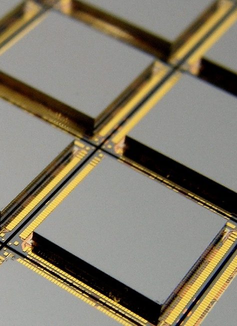
TC: The bond line is where you’re creating a medium to stick the two wafers together, sort of a window frame if you will. You’re aligning those two window frames against each other.
BM: The importance of bond line width is that it’s unused space for your device. The larger the bond line width, the fewer die you can get on a wafer. If you have a very small device, that can be a large effect. If you have a very large device, a wider bond line might be OK because, relatively speaking, it is not taking up too much space on the wafer. It is also a cost thing in the die level pricing because the more die you can get on a wafer, the less the cost of the device.
Which types of bonds are used most often at Atomica?
ES: There are categories at a high level. You’ve got a temporary bond, which is something we’re doing during the manufacturing process just to allow us to handle the wafer or process a thin wafer, for example. And then you have permanent bonds which are functional in the final product.
BM: We use these six bonds relatively regularly [see the table below]. We have current programs running each of them. We do temporary wax bonds regularly as well. We have done other types of bonds in the past and we’ve entertained doing others as well. But these six are the ones that we know the most about and we have the most experience with.
| Bond Type | Hermeticity | Vacuum | Temp (°C) | Difficulty | Bond Line Width (μm) | Bond Cost |
|---|---|---|---|---|---|---|
| Low temp metal alloy | Yes | High | 200 | Low | 100 | $$$ |
| Si fusion | Yes | High | 1050 | High | - | $$ |
| Glass frit | Yes | Medium | 420 - 440 | Medium | 400 | $ |
| Anodic | Yes | High | 370 | Medium | 50+ | $$ |
| Au Au thermo-compression | Yes | High | 200 -300 | High | <100 | $$$ |
| Polymer | No | No | 200 | Medium | 200 | $$ |
| Low temp metal alloy | Yes | High | 200 | Low | 100 | $$$ |
A low temp metal alloy bond is a proprietary one we’ve developed here. Basically, we have two different metal elements that come together. We heat that during the bond process while pressing and they form an alloy that is much stronger and has a much higher melting point than the bond temperature. So, we bonded around 200 C, and then it can withstand up to about 500 C after that without reflowing or moving.
The silicon fusion bond usually involves silicon to silicon or more frequently, silicon to silicon dioxide. You have two surfaces that are extremely flat and extremely low roughness, you bring them into contact with each other, and then you anneal them at a high temp. They fuse into one material.
The glass frit bond is a paste of sorts that has glass embedded in it as well as some solvents and various other chemistries. You screen-print that onto the wafer (just like you would a screen-printed T-shirt) into the bond line configuration. You bring the wafers together and heat them. That drives out all the solvents and turns it into a much more solid glass from that paste that you originally started with.
The anodic bond involves a silicon wafer and a special kind of glass wafer (borofloat) that has a lot of salt ions. You bring the wafers together and apply a very high voltage across those two wafers. You get an ion migration across the interface and the wafers fuse together. It’s a very high-strength bond that can be done relatively easily – a very good bond when you can allow for one of the wafers to be glass.
A lot of people do gold-gold (Au-Au) thermocompression bonds. One of the challenges is that you have to apply a large amount of force to get that bond to work properly. You also have to know how to prepare the surface properly. We have our own proprietary way of making a gold-gold thermocompression bond work better than just the kind of standard approach. The bond is good but it does add some complexity, which is why that’s one of the higher cost bonds (also because it’s gold which is a relatively expensive material).
With a polymer bond, you’re using some kind of polymer, like a glue. You pattern that polymer into the shape of the bond line that you want to use, press the wafers together, and drive out the solvents from that glue to solidify the polymer.
Even within some of these bonds, there are different types. For instance, there are many types of polymers. We have expertise in choosing which polymer is the best to use and how you would apply that polymer to the wafer.
What factors affect the choice of bond?
TC: That table shows six different bonding technologies. Some can be hermetic bonds or can hold a vacuum. It shows bonding temperature. These are very important pieces of information to have when you have wafer level packaging applications. For example, microbolometer infrared camera sensors – they have a certain material set that can’t be exposed to temperatures above 200°C. In that case, the low temperature metal alloy bond would be the candidate to explore. So, the type of bond depends on the end application and material set. Cost is a consideration as well.
BM: Topography on the wafer surface is also a factor to consider (such as bond pads coming out underneath the bond line). Something like a silicon fusion bond is not going to be able to overcome any topography on the bonding surface. You can have zero; it will not work if you have anything more. But a polymer bond or a glass frit bond can overcome some topography. We also have our own proprietary bonds, such as the low temperature metal alloy bond, which allows us to overcome some of that topography while still maintaining a very high vacuum, relatively narrow bond width, and a low temperature.
We have experience developing other bonds. We’ve actually come up with some bonds that allow for both compliance (with topography) and rigidity (for a very good, strong bond) at the same time for some specific biological applications where that is necessary.
There’s some additional complexity to some of the bonds or considerations that you need to make. For example, for the silicon fusion bond, you have to keep the surface incredibly pristine for that to function properly. That can present an integration challenge, depending on what the device is, to make sure that all the steps before the bond leave the surface of the wafer pristine. There are some cases where it’s relatively easy to do because maybe you’re not doing too much processing to that surface. But in cases where you’re making a complicated device and doing a lot of processing to that surface and then you have to achieve the silicon fusion bond, you just have to be careful and ensure that you have enough surface area for that bond to perform well.
TC: Brian mentioned a good point. It depends on when you are performing the bond. When the wafer has gone through lithography steps, metal deposition, and any processes, that surface is not going to be pristine. It’s going to be hard to keep it clean.
ES: I think it’s important for people to understand that every situation brings a different set of constraints. Sometimes you’ve got a thermal budget that you have to stay within because there’s some structure on the device that can’t go above a certain temperature. Sometimes you’re making a temporary bond and you need to be able to remove it easily during subsequent processing. Sometimes you are super concerned about the die size and therefore the cost of the device and so you can’t afford a thick bond line. And sometimes you might be concerned about how fragile the device is so you can’t apply a lot of pressure. You have to weigh all of these different constraints on the design considerations to choose what’s the best bond for a particular situation.
What does Atomica bring to the table regarding wafer bonding?
BM: I think Eric’s comment is a great segue – we’ve seen all these different bonds and we’ve seen what works in various situations. We can help walk the customer to not just the best approach for their application but also the lowest cost option for their device.
ES: I would say that maybe half of our programs, maybe more, require some type of bond, either a final bond or a temporary bond during fabrication. Any time you’re making sensors or photonics or bio chips, you’re going to need this expertise to make your final product. What are other people thinking in terms of the percent of our programs?
Stuart Hutchinson: Yes, I’d say at least half if you’re going to include temporary bonding as well. Wouldn’t you say so, Brian?

BM: Yeah, definitely.We also have some proprietary approaches that aren’t available anywhere else that allow for some unique benefits. Our proprietary bonds are patented; they are not available anywhere else and provide a unique solution.
ES: CMOS foundries, which are making transistors in very high volumes, don’t usually need to do bonding; it’s generally not a core competency for them. Similarly, these bonds often require materials that are not CMOS compatible. That limits the number of facilities where you would customarily make these types of bonds.
Another factor: what size wafers are you dealing with. It’s one thing to bond wafers at six-inch – we’ve been doing that for 20 years – but being able to do it at eight-inch. This introduces another level of complexity because you have much larger surface areas and you’ve got to have more uniformity across the wafer. There aren’t that many places in the world that have the expertise, the bonders, the chemical-mechanical polishing (CMP), electroplating, and all the other tools necessary to create good bonds on eight-inch wafers in a production foundry environment.
Do you have any projects with particular challenges that you would like to mention?
ES: Yeah. Brian, you could talk a little bit about Program X which introduces the need for topography, through silicon vias that can connect to the device, and a high hermeticity requirement. That’s a challenging set of constraints plus a thermal budget, too.
BM: Yeah, a little bit of everything in that case. We had a lot of constraints and also some cost concerns. Fitting all those constraints into place and figuring out how to integrate it into their device in a way that’s cost-effective, space-saving, high reliability, and high yielding is a challenge. We worked through that with the customer, making sure that we’re considering all of their constraints and finding the best solution for them.
Any other comments in closing?
ES: Yeah. The semiconductor industry, in general, is moving to a world that will require more and more of what we call 3D heterogeneous integration. Moore’s law is slowing down. We’re now at the point where the gate on a leading-edge transistors is less than three nanometers in size – that’s only like 10 atoms wide! Can you make them much smaller than that? With this limitations of continued scaling of traditional semiconductor manufacturing, we’re all starting to think… “if we can’t go smaller and smaller, how do we go vertically”? How can we stack devices so we can continue to keep reducing size and take advantage of the economics and the manufacturing advantages of semiconductor wafer processing? So, we’re seeing more and more devices stacked vertically.
We do a lot of work on CMOS wafers where post-process the wafer to and either add some additional functionality or bond something on top of it. We believe the industry is going to need more and more bonding to create these 3D structures that afford smaller devices, more functionality, a smaller footprint, better economics, and all of the things that you expect out of the electronics industry.