How is MEMS different than CMOS?

In this Article
- How are CMOS and MEMS fabs different?
- What materials cause issues for CMOS fabs?
- How does Atomica handle these materials?
As the world grows increasingly reliant on electronic devices, there is a constant push for the development of more advanced and specialized semiconductor technologies. These advancements often require materials outside the traditional “CMOS-friendly” palette to meet the unique needs of applications such as sensors, biochips, and various Micro-Electro-Mechanical Systems (MEMS).
CMOS vs. Non-CMOS Fabs
There is a significant distinction between CMOS and non-CMOS fabs. While CMOS (Complementary Metal-Oxide-Semiconductor) technology is extensively used in creating integrated circuits for microprocessors, memory, and other digital logic circuits, many specialized devices require materials and processes that are not CMOS-compatible.
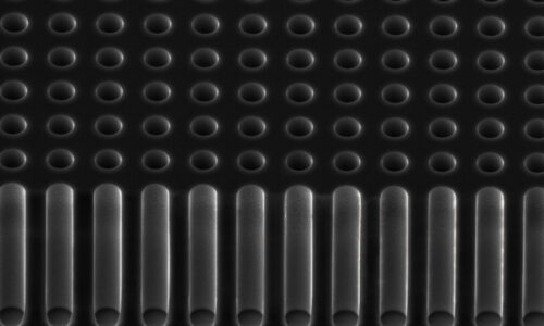
Manufacturing devices like sensors, biochips, and other MEMS often requires the use of non-standard materials and techniques. The challenges in using these materials lie in the potential risks they pose to the CMOS environment due to factors such as diffusion and contamination.
Risks of Non-CMOS Materials in CMOS Fabs
Magnetic materials, high-mobility metals, alkali metals, certain polymers, heavy metals, III-V semiconductors, piezoelectric materials, reactive compounds, and additional noble metals are among the broad range of materials used in non-CMOS applications.
These materials can create several complications if introduced into a CMOS fab, including:
- Disruption of device operation and measurement tools
- Leakage or shorting if they diffuse into silicon
- Device instability due to easy diffusion into SiO2 and silicon
- Outgassing or contamination of the CMOS process
- Creation of deep-level traps in silicon causing leakage currents and affecting device performance
- Integration challenges due to differing temperature, contamination risk, and lattice structure
- Contamination risks due to specific processing conditions
- Disruption of the properties of CMOS devices.
In essence, these materials can severely hinder the performance of CMOS transistors if even a trace remains in a chamber, limiting the number of fabs willing to work with them.
The Atomica Advantage
This is where Atomica comes in. As the leading MEMS foundry in the U.S., Atomica is perfectly suited to work with companies that need to utilize these materials. Since we do not produce transistors, we are not at risk of contaminating CMOS devices. Additionally, our 20+ years of experience and knowledge in working with these materials allows us to safely and efficiently accommodate the diverse requirements of our clients.
Here’s a snapshot of how Atomica can handle the challenges of non-CMOS materials:
| Material Type | Examples | Risks in CMOS Fabs | Atomica Approach |
| Magnetic Materials | NiFe | Disrupt device operation and measurement tools | Extensive experience with magnetic materials in a non-CMOS environment |
| High-Mobility Metals | Au | Cause junction leakage or shorting if they diffuse into silicon | Specialized handling and prevention measures to control diffusion |
| Alkali Metals | Na | Diffuse easily into SiO2 and silicon, leading to device instability | Utilizing alternate materials and strategies to minimize risk |
| Certain Polymers | Polyimide | May outgas or have components that contaminate the CMOS process | Implementing strategies to prevent outgassing and contamination |
| Heavy Metals | Pb | Create deep-level traps in silicon, causing leakage currents and affecting device performance | Handling and containment protocols to prevent contamination |
| III-V Semiconductors | GaN, InP, GaAs | Their differing temperature, contamination risk, and lattice structure make integration challenging | Long-standing expertise in integrating III-V semiconductors |
| Piezoelectric Materials | AlN, PZT, LiNbO3, LiTaO3 | Require specific processing conditions and contain elements that can potentially contaminate CMOS devices | Experience with diverse piezoelectric materials and associated processing conditions |
| Reactive Compounds | Phosphorus compounds | Disrupt the properties of the CMOS devices | Handling processes designed to prevent disruption of CMOS properties |
| Additional Noble Metals | Ag, Pt, Pd, Ru | Can diffuse into silicon and disrupt device operation | Extensive experience handling noble metals in a non-CMOS setting |
At Atomica, we are ready to help you innovate, and our specialized non-CMOS foundry capabilities are unmatched. As the world of semiconductors continues to evolve, you can count on us to enable your success by ensuring the safe and effective use of the full richness of the periodic table.