SiOBs: What are Silicon Optical Benches and their benefits?

Learn the following in this post
- What are silicon optical benches (SiOBs)?
- How SiOBs relate to traditional optical benches.
- How silicon optical benches are made.
- What are the benefits of using SiOBs for optical integration?
- What is Atomica’s experience in creating SiOBs?
Silicon optical benches (SiOBs) are named after the benchtop optical benches that scientists have used to study light for more than a century. Why are SiOBs so useful? Because they precisely align each optical component in the x, y, and z dimensions. SiOBs are therefore critical for directing photons through an optical obstacle course to achieve a desired function — whether communicating, sensing, measuring, imaging, or performing other photometric studies. But their greatest benefits in improving costs, precision, and size come from moving this integration to the wafer level.
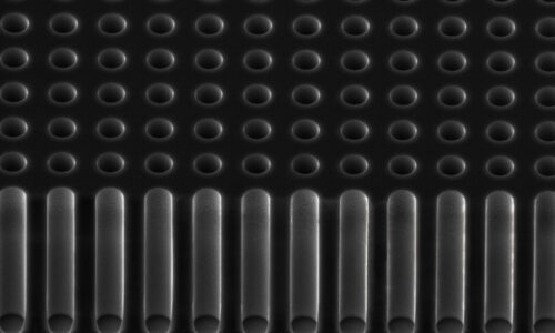
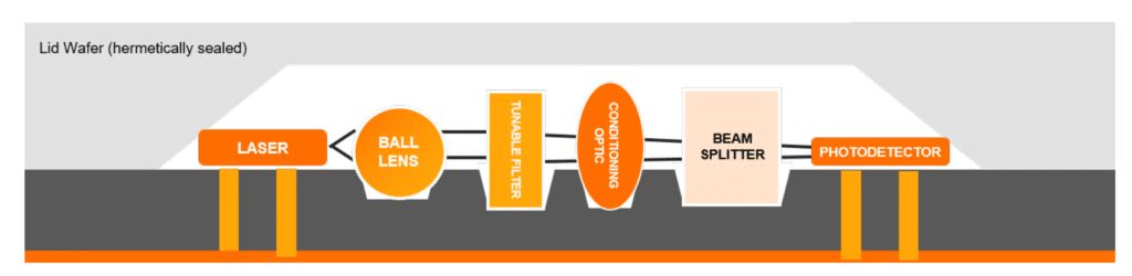
Unlike traditional optical benches, which rest on a specialized table or “breadboard”, an SiOB employs a piece of silicon as the “table”. Discrete optical elements such as lenses, lasers, mirrors, and beam splitters are placed into kinematic cavities or pits in the silicon that are specially designed to precisely hold each element in its correct 3D position. Some optical elements, such as mirrors, can be formed into the surface of the silicon itself.
Think of a high-precision 3D jigsaw puzzle, and you’ll be picturing an SiOB. The prime directive of an SiOB is channeling, handling, and guiding light to its destination.
SiOBs are fabricated with wafer-level semiconductor processes, including nanometer-scale lithographic patterning of features. This unprecedented precision combines with advances in etching, film deposition, wafer-level bonding, and sub-micron precision pick-and-placing of components to deliver a range of benefits.
Benefits of SIOB:
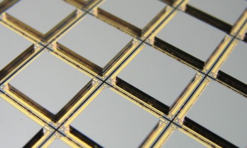
Size: By making benches through semiconductor-wafer processes, optical elements can be packed onto chips with sub-micron precision and density. The resulting optical “engines,” sensors, and transceivers are a fraction of the size of conventionally assembled optical systems— “staggeringly small”, as Richard Feynman would have said.
Cost: Because SiOBs are made on wafers, they can be fabricated on a massive scale. Each wafer can contain many thousands of identical devices. At this economy of scale, the cost-savings from wafer-level manufacturing cannot be beat. Wafer processes also enable automated testing and inspection, further reducing your costs versus serial testing.
Precision: (Nano)lithographic feature precision plus the latest advances in placement technology ensure that your optical elements are placed with very tight tolerances. The benefit to you? High fidelity in the manufacturing of optical systems.
Low loss: SiOBs can be engineered for low loss by leveraging free-space optical paths or by coupling them to low-loss waveguides.
Hermiticity: SiOBs are commonly topped with a lid wafer using wafer-level bonding techniques. This strategy positions you to create hermetic (airtight) cavities for the entire optical system, ensuring high reliability and lifetime protection from environmental hazards such as moisture, oxygen, and dust, which can degrade the performance of many optical elements.
By looking “under the hood” of SiOBs, we’ve gotten a sense of how these underappreciated components are driving today’s technology revolution. Next time, we’ll explore optical transceivers, which are the highest-volume market for SiOBs.
At Atomica, we produce millions of SiOBs every year, thanks to our unmatched expertise, proprietary processes, and extensive tooling for integrated micro-optics. For these reasons, Atomica is the leading one-stop shop — from design to development to manufacturing — for companies needing customized SiOBs on both 150-mm and 200-mm wafers.