Machines Can See: MEMS and the Dawn of Computer Vision

Learn the following in this post
- Emerging applications for computer vision
- What technologies have been used to help computers see?
- How MEMS help advance vision technologies
- What expertise does Atomica bring to computer vision?

The age of computer vision is truly dawning. The technology for remote sensing across the electromagnetic spectrum has matured to the point that it is now practical, and it is almost cost-effective enough to adopt throughout the economy.
The ability of machines to see will usher in new waves of innovation and economic growth akin to, and no less significant than, the creation of the first machines that translated fuel into motion.
In 1698 England, Thomas Savery built the first steam engine and used it to pump excess water out of coal mines. It was terribly inefficient, but improved steam engines enabled steamboats (1783), machine-powered textile mills (1790), locomotive railways (1804), and eventually, the delivery of motion anywhere man desired without reliance on rivers, humans, or animals. Recent improvements in computer vision will herald a similar era of economic transformation.
Emerging applications for computer vision
Emerging applications for computer vision are as vast as the human imagination. They include:
- Advanced driver assistance systems (ADAS)
- Autonomous vehicles
- Crop and forest monitoring systems
- Automated inspection and quality control systems
- Myriad defense applications (missile guidance, threat detection, perimeter monitoring)
- Navigation drones, UAVs, and aerospace systems
- Factory automation
- Metrology systems and analytical instruments
- Household robotics
- Surgical devices
- Security and surveillance systems
- Medical diagnostics

Computer vision technologies today utilize five segments of the electromagnetic spectrum (see table below) to create 3D images of the world around them.
Traditional technologies for computer vision
Most of these technologies were invented 80 or more years ago. It is only with recent improvements in processing power, wafer manufacturing, and laser and sensor technology that these imaging systems can be packaged and deployed across everyday applications such as automobiles and smartphones.
The fusion of output from these different sensor types enables a more complete and resilient picture of our environment. The table below summarizes the major machine vision technologies across the electromagnetic spectrum.
| Technology | Wavelength (Frequency) | Trade-Offs | MEMS Roles | Invented |
|---|---|---|---|---|
| Ultrasound (sonar) | ~6.8mm(~50Khz) | Effective in the dark Short range Low speed Low resolution | Transducers | 1906 |
| Radar | 3-15mm (20-100Ghz) | Long range(200m+) High speed Insensitive to light Effective in the dark Low resolution | Switches Time delay units Filters Waveguides | 1935 |
| Thermal Imaging | 8-14um | Long range(200m+) Effective in the dark Only detects thermal emitters | Micro-bolometers Micro-lenses Wafer-level packaging (Hermetic) | 1929 |
| Laser Imaging (LIDAR) | 800-1550nm | Good range(100) Effective in the dark High resolution | Mirrors Lenses Waveguides Optical benches | 1960 |
| Visual Cameras | 400-800nm | High resolution Medium range(50m) Ineffective in the dark No range information | Lens actuators (autofocus, stabilization) | 1816 |
| Ultrasound (sonar) | ~6.8mm(~50Khz) | Effective in the dark Short range Low speed Low resolution | Transducers | 1906 |
| Radar | 3-15mm (20-100Ghz) | Long range(200m+) High speed Insensitive to light Effective in the dark Low resolution | Switches Time delay units Filters Waveguides | 1935 |
How MEMS help advance vision technologies
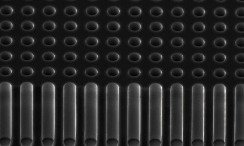
MEMS and related wafer-level manufacturing capabilities play a central role in advancing these vision technologies to the point of widespread adoption. For example, thermal imaging systems have progressed from single-pixel thermopiles used to detect icebergs from a distance over 100 years ago to today’s vanadium-oxide MEMS microbolometer pixel arrays, which can measure microscopic changes in resistance to sense thermal energy at a distance and thus paint a picture at night.
Similarly, scanning MEMS micro-mirror arrays can now raster a scene with high-powered lasers to paint a picture of surrounding objects by measuring the time delay of the lasers’ reflections.
Atomica’s role in computer vision
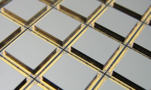
Atomica has partnered with its customers for nearly 20 years to help design and manufacture the critical components of these systems, including mirrors, lenses, and hermetic cavity packages—all done at a wafer-scale to assure semiconductor precision and wafer-level economics.
Click here to contact Atomica and discuss how we can help enable the next generation of computer vision systems.


