
MEMS Optical Control Platform
Representative structures: micromirrors · comb-drive actuators · diaphragms and tunable membranes · microlenses · silicon optical benches · wafer-level optical packaging
A broader foundation for MEMS development: Atomica’s MEMS expertise extends beyond optical control.
Our platforms for sensing, biotechnology, thermal management, and integration support a wide range of MEMS devices, with application-specific offerings detailed in their respective sections.
For designs that require a different combination of functions or structures, Atomica can draw on shared building blocks such as actuators, diaphragms, interconnects, and wafer-level packaging.
We adapt these to the device’s requirements and develop additional process steps where needed, giving custom MEMS programs an established foundation for development and production.

Building MEMS for AI infrastructure?
If your MEMS device is going into AI hardware, start here.
Why Atomica?
A manufacturable path from prototype to production
Atomica is a U.S.-based microfabrication foundry that turns advanced device concepts into manufacturable, scalable hardware — and its advantage is not a single process but a system that de-risks the path from first prototype to volume.
30,000 sq ft cleanroom · Class 100 · ISO 9001 certified · ITAR registered · Santa Barbara, USA
1
Engineering Collaboration
Atomica works as an engineering partner across design, materials, fabrication, and testing, bringing diverse expertise together to optimize each micro-scale device. That collaboration is what yields better products, lower cost, faster time-to-market, and quicker adaptation to emerging technologies.
2
Process Standardization
Standardized processes give a clear framework for fabrication, scaling, and quality control. This is what delivers the consistency, quality, and efficiency that reliable, high-performance microdevices require — while supporting regulatory compliance and continuous improvement.
3
Modeling & Simulation
Atomica evaluates designs before fabrication using physics-based modeling, FEA, CFD, AI, and multiphysics simulation. Simulating first reduces prototype iterations, lowers cost, identifies risks early, and improves first-pass success across photonics, sensors, biotech devices, MEMS, and integrated microsystems.
4
AI Optimization (FabOps)
Atomica’s FabOps system applies AI and advanced analytics across wafer inspection, metrology, fab control, and project execution. By integrating equipment, process flows, pricing, projects, and manufacturing — with real-time visibility, lot tracking, and change control — it reduces risk and accelerates programs from prototype to scalable production.
5
Fab Technology
Atomica operates a 30,000 sq ft, class-100 cleanroom near Santa Barbara, California — ISO 9001 certified and ITAR registered. Its full in-house process suite spans photolithography, deposition, dry and wet etch, bonding, plating, metrology, testing, dicing, and planarization, purpose-built for rapid prototyping and scalable production.
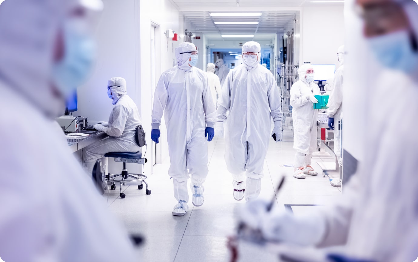
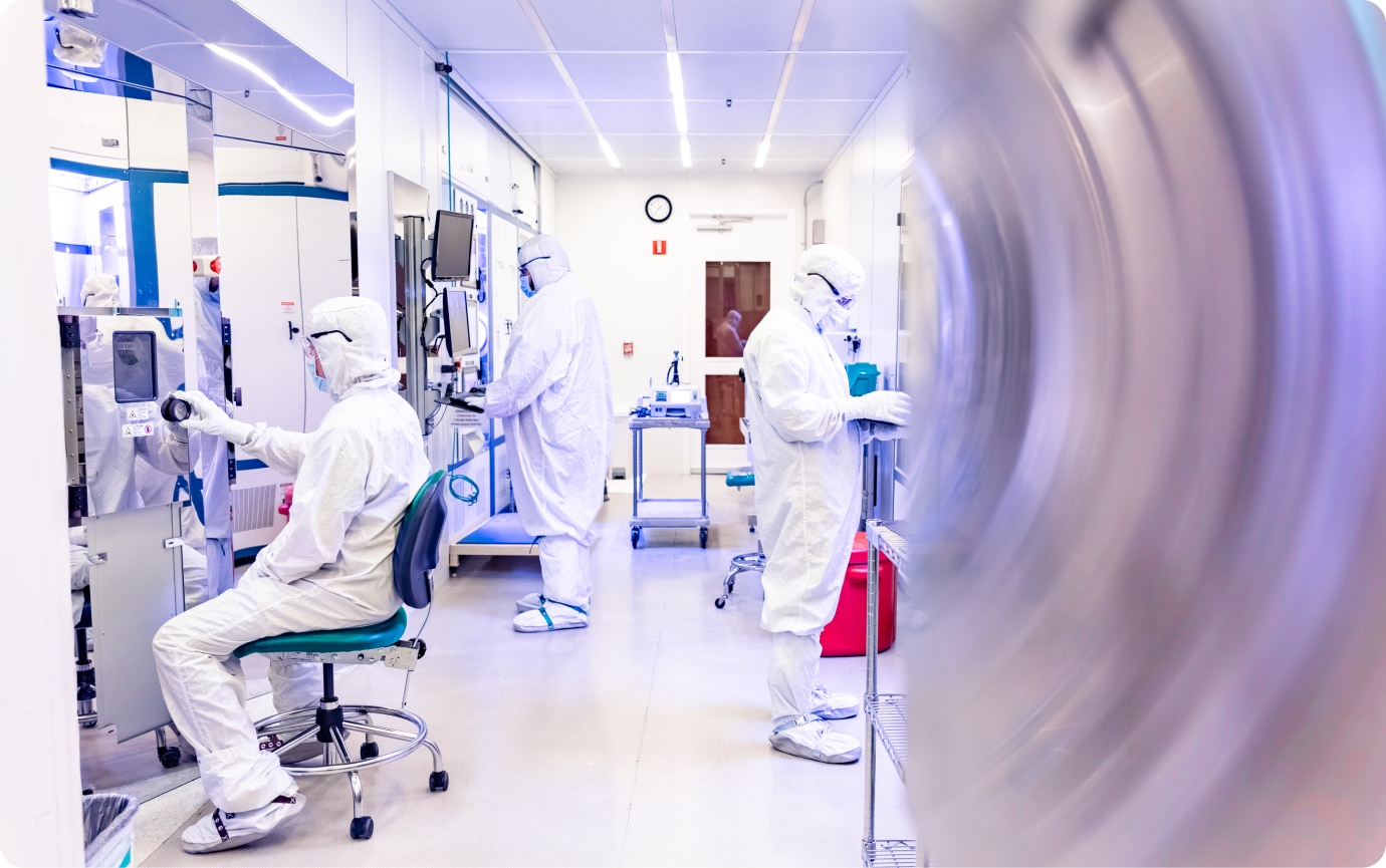
Explore Atomica’s in-depth resources to navigate modeling and simulation, rapid prototyping, scalable production, and fab evaluation — all with expert insight.
Rapid Prototyping Services at Atomica
Uncover our efficient process that turns ideas into working prototypes swiftly, helping you bring innovations to life quickly.
Scaling Production with Atomica’s Expertise
Explore how our advanced production methods ensure consistent, high-quality, and cost-effective results at every stage of scale.

Inside Atomica’s Advanced Fab Technology
Take a detailed look at our high-tech capabilities, engineered to support complex, precision-driven microfabrication.

Selecting the Right Fab for Your Project
Our Fab Evaluation Guide outlines essential criteria, ensuring your project is matched to the best fabrication partner.
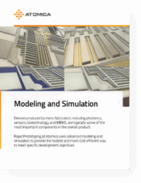
Simulation-Driven Microfabrication
See how modeling and simulation improve performance, lower cost, shorten timelines, and drive better outcomes.