What you will learn in this ebook?

Discover the myriad benefits that wafer level packaging affords over traditional semiconductor and component packaging approaches.
Learn about the numerous applications that benefit from well executed wafer level packaging.
Take a comprehensive look at the major steps in designing and manufacturing wafer level packaged MEMS devices.
What is Wafer Level Packaging?
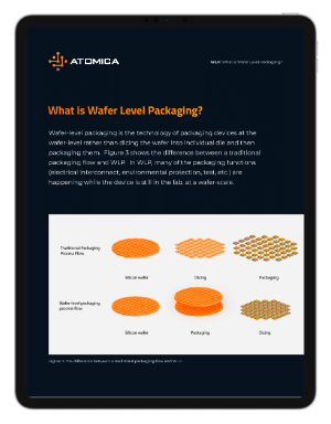
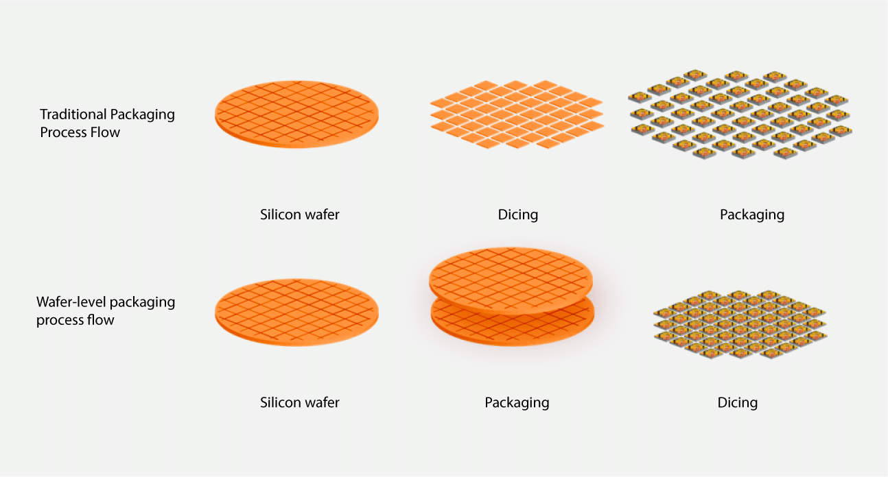
Wafer-level packaging is the technology of packaging devices at the wafer-level rather than dicing the wafer into individual die and then packaging them. The figure below shows the difference between a traditional packaging flow and WLP. In WLP, many of the packaging functions (electrical interconnect, environmental protection, test, etc.) are happening while the device is still in the fab, at a wafer-scale.
Benefits of Wafer Level Packaging
01. Size
By using semiconductor-wafer processes and mitigating wasted space, wafer level packages can reduce the footprint size versus conventional semiconductor packages. Furthermore, the ability to stack and directly interconnect elements in the vertical dimension affords even greater volume savings.
02. Cost
WLP benefits from the economies of scale of wafer-based fabrication processes. The cost per unit is minimized since each wafer has thousands of identical devices fabricated in parallel. Further, automated inspection, test, and burn-in at the wafer scale dramatically decreases costs.
03. Heterogenous Integration
3D integration of multiple die, MEMS devices, sensors, or even optical components at the wafer level increases functionality and allows for the use of disparate manufacturing processes, which would have otherwise been suboptimal to integrate in CMOS.
04. Speed and Noise
WLP and 3D integration can reduce signal lengths normally required with conventional packaging or wire bonded devices. Shorter signal paths exhibit less noise, greater signal integrity, and thus can support higher speeds due to the reduced parasites.
05. Hermeticity
Systems that require inert environments like SiOBs are commonly topped with a lid wafer using wafer-level bonding techniques, allowing a hermetic and even vacuum cavities for the entire system. This environmental benefit can help many types of device systems improve performance, reliability, and lifetime.
WLP Applications
01
IoT Sensors
Microphones, pressure sensors, gas sensors, chemical sensors, accelerometers, and gyroscopes are essential for the all sorts of IoT devices. They all benefit from various forms of WLP to seal cavities, enable smaller footprints, or enable heterogeneous integration of multiple die.
02
Infrared Imaging and Microbolometers
Infrared imaging and sensing systems are seeing increased adoption for 3D sensing, night vision, and spectroscopy. Many of the elements in IR systems can benefit from WLP including microbolometers, micro-optics, and even the lens elements.
03
LiDAR
Packaging laser emitters, scanning mirrors, and image sensors into smaller and smaller form factors while also reaching further into the IR to maximize signal and minimize safety issues pushes the capabilities of technology.
04
MicroMirrors
MEMS mirrors are used in many applications including telecom optical switching, LiDAR, spectroscopy, and micro-projectors (such as DLP). The need for hermeticity and optical transmission at specific wavelengths while having diverse scanning requirements makes WLP of these devices a multivariate problem.
05
Optical Telecom
Wafer level design of variable optical attenuators, switches, and photonic integrated circuits (PIC) can enable higher performance and reduced size and cost with high level parallel integration.
06
Wafer Level Optics
Fly-eye microlens arrays and fabricating imaging systems for cutting-edge sensor applications benefit from fabricating at wafer level if device size and production volume benefit from wafer scale development.
07
Resonators/Switches
There are many innovative MEMS architectures that resonate or switch. Over the past two decades the performance, size, and costs have come down dramatically due to parallel manufacturing that reduces the handling, increasing yields compounding the economic benefits. These devices almost universally benefit from WLP.
08
Microfluidics
Microfluidic chips are advancing many aspects of medical diagnostics, genomics, proteomics, and even stem cell therapies. These devices may integrate a channels, pumps, micro-well arrays, mixers, or sensing elements. It’s very common for these chips to comprise multiple wafers that must be bonded and packaged at the wafer level.
About the company
We are experts at navigating the design trade-offs to deliver a product that meets technical and economic specifications. We have been developing and manufacturing MEMS for nearly 20 years. Our extensive experience spans the full spectrum of MEMS including optics, sensors, relays, RF switches, and microfluidic biochips. Atomica (formerly IMT) partners with our clients to get the best of both worlds – world-class development and high-volume manufacturing.