Exploring MEMS: The Tiny Tech Revolutionizing Our World
Learn the following in this post
- What are MEMS?
- What are MEMS applications?
- How are MEMS made?
- What are the advantages of MEMS?
- What are the future of MEMS

The Basics
Microscopic versions of conventional full-size mechanical and electrical components are being fabricated and combined into minuscule packages, allowing smartphones, wearable electronics, and automobiles to do amazing things. This is the world of microelectromechanical systems (MEMS).
Depending on application and geographical location, MEMS might be referred 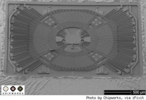
Although fabricated in a manner similar to semiconductors or integrated circuits, MEMS are distinct in that they have some sort of mechanical function allowing the device to interact with its surroundings. Some MEMS incorporate moving parts (such as cantilevers, springs, or pressure-sensitive diaphragms) while others do not (RF filters, BAW filters, photonics, and optical benches).
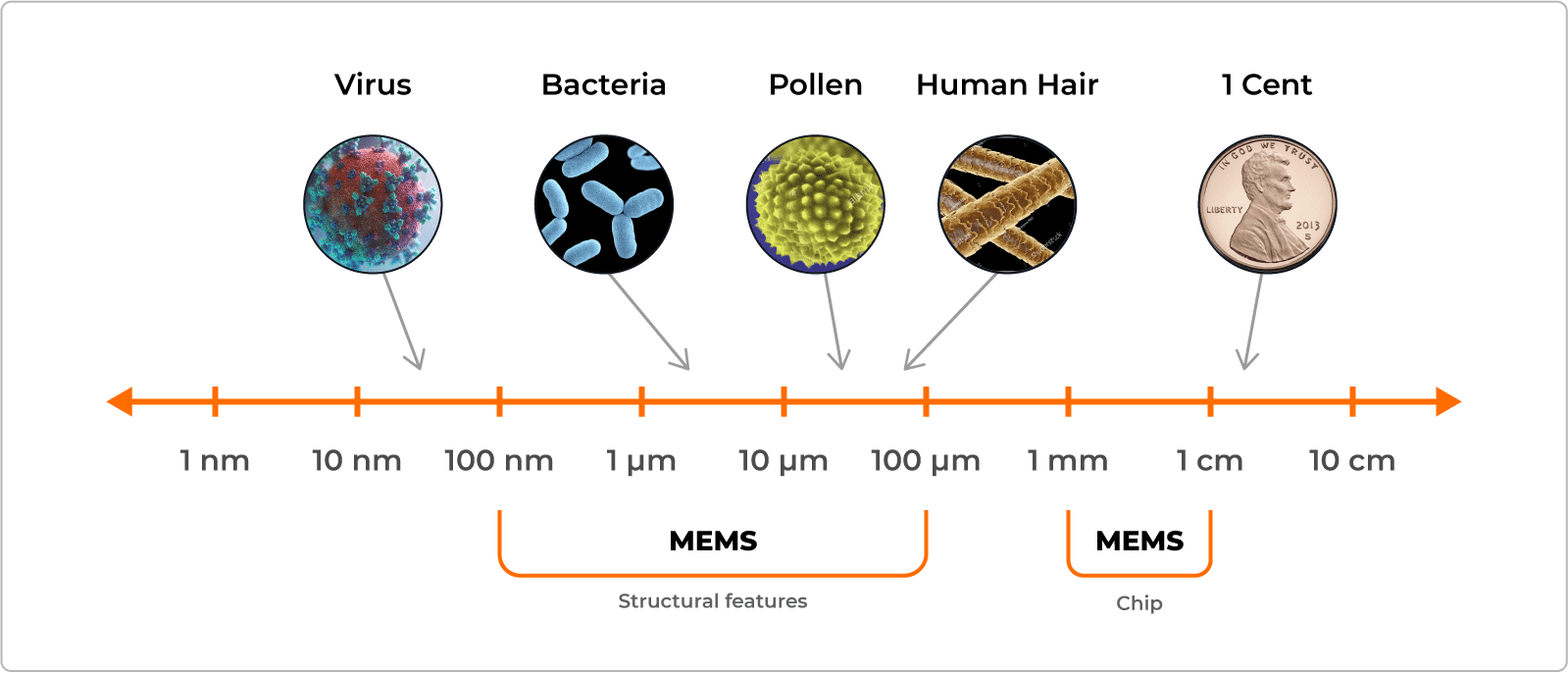
Microstructures were first envisioned in the 1960s. The 1970s brought several key developments including the first microprocessor, bulk-etched silicon wafers, and the first micromachined inkjet nozzles. In 1982, Kurt Petersen touted silicon’s mechanical properties, calling it “a high-precision high-strength high-reliability mechanical material, especially applicable wherever miniaturized mechanical devices and components must be integrated or interfaced with electronics.” During the 1990s, the different types of MEMS expanded quickly (including the first accelerometer), and the growing infrastructure for MEMS design and fabrication pushed mass-produced devices to commercial viability. Optic- and Bio-MEMS emerged in the 2000s, and today there is a wide proliferation of many categories of MEMS.
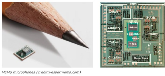
What are MEMS applications?
MEMS serve in a wide array of functions, including as sensors, actuators, switches, and energy sources in areas such as optics, audio, radio, fluidics, and other physical phenomena
Some of the more common and noticeable uses are:
- Inertial sensors
- Pressure sensors
- Magnetic sensors
- Micromirrors
- Micropumps
Inertial sensors include accelerometers and gyroscopes used individually or combined in sets. Accelerometers measure straight-line acceleration, typically using a mass on a spring to detect inertial forces. Gyroscopes detect rotation or angular change. MEMS gyros usually employ paired objects that vibrate like a tuning fork: when the vibrating objects are rotated, a measurable force is created as the masses move out of plane due to the Coriolis effect. A large number of inertial sensors support automotive safety as triggers for airbags and active seat belts. Inertial sensors are also found detecting motion and orientation in smartphones, inertial navigation systems, and vehicle stability control systems.
MEMS pressure sensors compare the pressure in a gas or fluid on one side of a silicon diaphragm to a set reference or ambient pressure on the other side. There are several different pressure sensor technologies, such as piezoresistive, capacitive, and inductive. As an example, piezoresistive pressure sensors detect the strain caused by the difference in pressure that results in a measurable change in electrical resistance in the diaphragm materials. These technologies provide options to serve a wide variety of applications, including automobiles (engine performance control, tire pressure monitoring), medical devices (blood pressure and respiratory monitoring), and drones (altimeters).
Magnetic sensors (or magnetometers) determine the strength and direction of a magnetic field using the Lorentz force, which is felt when a looped electrical current passes through a magnetic field. This force causes the loop to flex in proportion to the strength of the field, and these movements can be detected either electronically or optically. MEMS magnetic sensors are used in areas such as electronic compasses, vehicles (anti-lock brakes, cruise control), and security systems.
MEMS micromirrors consist of microscopic mirrors sitting on pivots. The mirrors are usually set in an array in which the center-to-center spacing may be as little as five to ten microns. Using electromagnetic or electrostatic actuation, each mirror’s position can typically be toggled on (allowing light to flow out to some destination) or off (with the light reflected to a heatsink). Intermediate light levels can be achieved by fluttering the mirror to vary the amount of time spent in the on position. Micromirrors are key to digital projectors located in many conference rooms and digital cinemas across the country. MEMS mirrors are also used for laser beam steering (for instance, in LiDAR) and as switches in fiber-optic communications.
The earliest and most recognizable use of the micropump comes in the form of inkjet technology. An empty cavity sits behind each of the nozzles in the print head. Ink flows into the cavity and, when heated by minuscule heating elements, is ejected from the nozzle onto the waiting paper. Automated drug delivery systems also commonly employ micropumps.
| MEMS devices… | …and where they can be found |
|---|---|
| Inertial sensors (accelerometers, gyroscopes) | Aerospace, missile guidance, drones, autonomous vehicles, robotics, smartphones, medical devices (e.g., sleep monitoring, pacemakers), airbag sensors, navigation systems |
| Magnetic sensors | Industrial controls, security systems, automotive (e.g., speed control, anti-lock brakes), consumer electronics, appliances |
| Pressure sensors | Engine control, industrial automation/process control, health monitoring (blood and respiratory), tire pressure monitoring, HVAC, auto powertrains, drones, smartphones |
| Gas sensors | Pollution monitoring, medical devices, alcohol detection, manufacturing process control, fire and safety systems, HVAC, smart buildings |
| Flow sensors | Utility meters, industrial systems, CPAP and respiratory systems, automotive |
| Thermal sensors and imagers (e.g., bolometers) | Night vision, fever detection, autonomous vehicles, surveillance systems, fire detection, HVAC, smart buildings, predictive maintenance, drones, process control |
| Humidity Sensors | Agriculture, industrial automation and process control, HVAC, smart buildings |
| Transducers | Ultrasound imaging, automotive subsystems, sonar, touch sensing, fingerprint readers |
| Microactuators | Cell sorting, microcamera autofocus and image stabilization, disc drives, semiconductor testing/probing, atomic force microscopes |
| MEMS switches and relays | 5G wireless communication, radar , antenna arrays, test and measurement systems, automobiles, medical imaging, semiconductor testing |
| Radio frequency (RF) filters | Wireless communications (smartphones, radios, base stations , satellites, aerospace), medical diagnostics (COVID-19 testing) |
| Resonators | Oscillators and clocks for electronics, medical and analytical instruments, RF filters/tuners |
| Photonic circuits (couplers, SiOBs, waveguides, gratings) | Optical communications, medical imaging, LiDAR, 3D sensing, metrology, analytical instruments, quantum computing, RF photonics |
| Micromirrors | Optical communications, LiDAR, 3D sensing, displays, AR/VR, medical imaging (OCT) |
| Microlens arrays | LiDAR, AR/VR, displays, cameras, 3D sensing, metrology |
| Microphones and speakers | Smartphones, computers, tablets, in-ear earphones, wearables, hearing aids, seismic exploration, consumer electronics |
| Micropumps | Drug delivery (nebulizers, insulin pumps, pain treatment, etc.), inkjet print heads |
| Microneedles | Glucose sensing, drug delivering, blood sampling, wearable health sensing |
| Microfluidics | Diagnostics, cell therapy, genomics/proteomics, organ-on-a-chip, chemical detection |
| Thru-silicon vias (TSVs), Interposers, and submounts | Interconnect for high-performance computing, quantum computing, high-density RF radios, optical communication transceivers, and other dense electronic systems |
| Chip-scale atomic clocks | Navigation systems (GPS), communication systems, precision timing systems |
| Energy sources | Microscopic fuel cells, supercapacitors, microbatteries, thermionic generators |
How MEMS are made
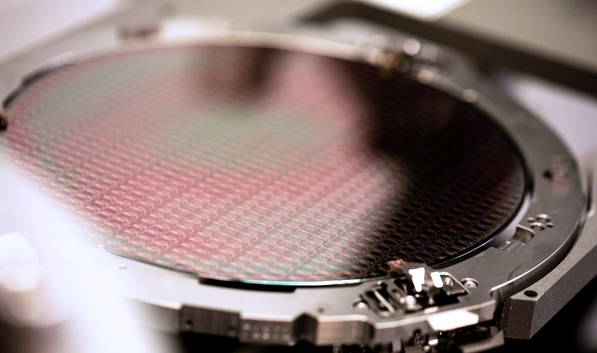
MEMS devices and integrated circuit (IC) chips are manufactured via similar processes. Both start on a foundational substrate wafer (typically of silicon or glass) and are then built up and sculpted through subsequent steps:
- Adding material layers through deposition,
- Patterning the surface through masks and photolithography, and
- Subtracting unwanted sections via etching.
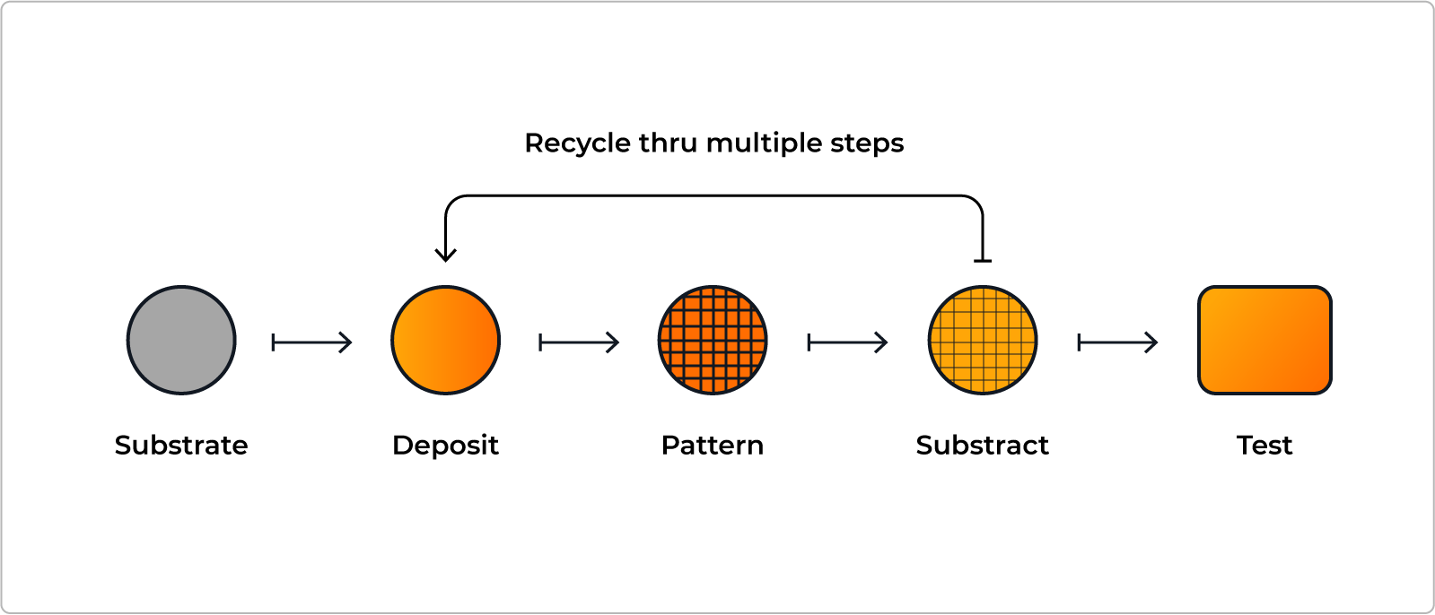
Four key aspects differentiate MEMS processes from IC: First, MEMS employ more diverse depositional materials such as piezoelectrics (for example, lithium tantalate, lithium niobite, and PZT) and noble-metal electrode layers (such as gold and silver). Second, to produce intricate three-dimensional structures, MEMS fabrication requires a broader assortment of process steps, including deep reactive ion etching (which results in near-vertical sidewalls), wafer-level packaging, and depositing very thin layers that may be less than one micron thick. Third, the shaping of a MEMS microstructure occurs both within the deposited layers and within the substrate.
Fourth, for MEMS processes, testing occurs as much in the physcial world as the digital. Most IC chips require only that they receive electrical current to determine whether their digital output passes or fails. MEMS, on the other hand, are made to sense or interact with physical parameters. Testing protocols, therefore, become more complex for MEMS than for IC chips. Accelerometers and gyroscopes must be moved, micromirrors must be actuated under a light source, and pressure sensors need physical pressure applied.
Advantages of MEMS
Regardless of the complexities of manufacture and testing, MEMS possess several key advantages over their larger macro-sized equivalents.
- Size is the most obvious benefit. MEMS can be installed in locations impossible for full-size components. Smartphones and electronic wearables would not be essential parts of daily life without these tiny machines. Self-driving cars would bristle with an impossible bulk of sensors. Certain modern tools and products would simply not exist.
- MEMS are fast. Electrical distances between components are short, cutting response time. Very small moving parts travel smaller distances and can attain higher frequencies.
- MEMS yield a level of performance and precision unattainable with conventional full-size components (for example, significantly reduced losses and a regime of sensitivity attuned to smaller quantities).
- With power consumption a small fraction of that for traditional components, there is considerably less demand on batteries for portable products.
- MEMS exhibit high reliability. Silicon materials can bear repeated flexure with very little fatigue and can offer an extremely long life under an incredible number of cycles.
- Although upfront research, design, and setup costs can be high, scalable mass production using batch techniques similar to the IC industry leads to very low per-unit costs for MEMS.
The future of MEMS
MEMS have secured a foothold in today’s industrial and electronic world – and are poised to play even more crucial roles in tomorrow’s innovations. These miniature components serve a wide range of functions in an even wider array of applications. Their size, speed, reliability, and low cost provide great value, and revolutions in fields such as 5G communications, IoT sensing, biochips, and autonomous vehicles will ensure exponential growth for the foreseeable future.


