Atomica announces new brand, $50 million tool acquisition
PRESS RELEASE
Transaction catapults Atomica (formerly IMT) to forefront of MEMS industry
SANTA BARBARA, CALIF. (PRWEB) MAY 11, 2021
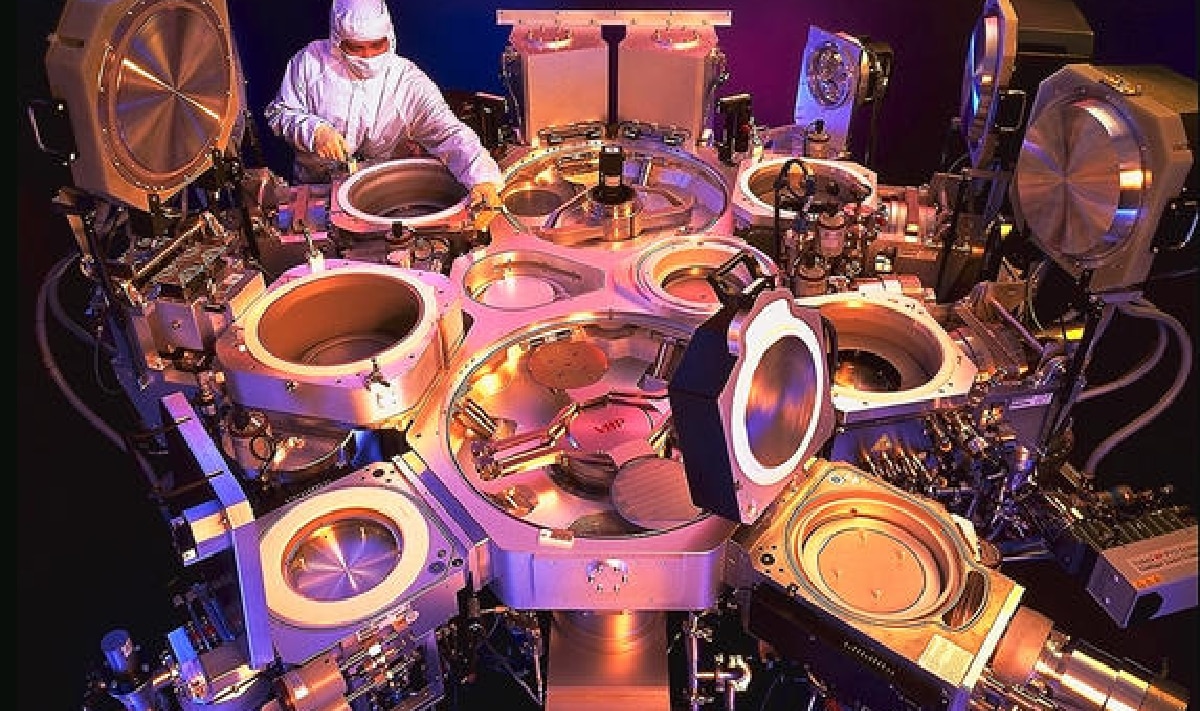
Atomica, Corp, a global leader in micro electro-mechanical systems (MEMS), has acquired $50 million of cutting-edge semiconductor processing tools. This massive capability upgrade advances Atomica to the forefront of the MEMS industry, supporting the domestic production of critical sensors, photonics, and biochips. The new brand signifies a repositioning of the company following major strategic changes over the past two years.
Atomica’s brand promise is to successfully commercialize its customers’ life-changing technologies in cloud computing, autonomous vehicles, cell therapy, molecular diagnostics, genomics, 5G, Internet of Things (IoT), and more.
“Our customers are on missions to cure disease and revolutionize sensing and communications. We are resolved to get them there,” said Eric Sigler, CEO of Atomica.
To help its customers successfully navigate the journey from prototype through volume production, Atomica leverages a unique collaborative methodology. Its business model is flexible, and includes bespoke process development, diverse materials, and a range of program sizes. Finally, it utilizes rigorous project management to optimize resources, mitigate risks, and deliver predictable results.
The new name, Atomica, reflects the company’s mission to help address major problems in the world by unleashing the power of MEMS. The company’s material science experts draw from the richness of the periodic table to engineer and manufacture innovative solutions. These MEMS components are typically a fundamental part or “atomic unit” of the groundbreaking products of Atomica’s customers.
Atomica has undergone a two-year transformation initiated with a change of ownership in late 2018, followed by a new executive team, improved systems and an 8” wafer line. The purchase of more than 300 state-of-the-art semiconductor processing tools marks a key milestone in the company’s transformation. It expands Atomica’s capability to develop and manufacture sophisticated micro devices. Examples of the new 200 mm-compatible equipment include:
- Applied Materials Endura PVD for precise sputtered films
- Veeco Phoenix atomic-layer deposition (ALD) system enabling atomic-scale high quality conformal coatings
- Evatek Evaporator for high-volume deposition of evaporated films and optical coatings
- Plasma-Therm High Density PECVD for high quality lower-temperature dielectric films with superior gap fill
- Plasma-Therm RIE etch cluster for a variety of production uses
- Multiple production-grade lithography systems from Suss and OAI
- Over 100 new advanced metrology systems including automated optical inspection
- Nearly a dozen new automated wet benches.
Complementing this new equipment is Atomica’s appointment of Rick Glasmann as Vice President of Process and Equipment Engineering. Mr. Glasmann is a world-class semiconductor executive with over 25 years of semiconductor equipment and operations experience. He most recently served as COO of Deca Technologies. He was previously an engineer with Applied Materials, followed by 20 years at International Rectifier (Infineon).
About Atomica
Atomica Corp. (formerly Innovative Micro Technology) unleashes the power of Micro Electro-Mechanical Systems (MEMS) to help solve the great problems of our time. Utilizing a uniquely collaborative approach to development and manufacturing, it partners with innovative companies to deliver breakthrough MEMS-based solutions in cloud computing, autonomous vehicles, cell therapy, molecular diagnostics, genomics, 5G, the Internet of Things (IoT), and more. Atomica is the largest MEMS foundry in the USA, serving customers from its 130,000 ft2 manufacturing campus (including a 30,000 ft2 class 100 cleanroom) in Santa Barbara, California. The company is ISO 9001 certified and ITAR registered. Its extensive experience spans the full spectrum of MEMS, including photonics, sensors, microfluidic biochips, and other micro components.