What are TSVs?

In this Article
- What value do TSV technologies provide?
- What are the benefits of custom vs standard TSVs?
- What are the key factors in manufacturing TSVs?
- What is the difference between TSV first vs. TSV last?
- Why is Atomica the best manufacturer of TSVs?
Envision a semiconductor landscape where interconnect density is maximized, signal integrity is flawless, and form factors are remarkably compact. At the core of these advancements is the transformative through silicon via (TSV) technology.
TSVs facilitate vertical electrical connections through silicon wafers, crucial for enabling advanced 2.5D and 3D IC integrations. This technology is pivotal in optimizing power efficiency, signal transmission, and thermal management in high-performance computing as demanded by AI, advanced consumer electronics, and cutting-edge medical devices. TSVs are driving the next wave of innovation in microelectronics, offering unprecedented opportunities for heterogeneous integration and miniaturization.
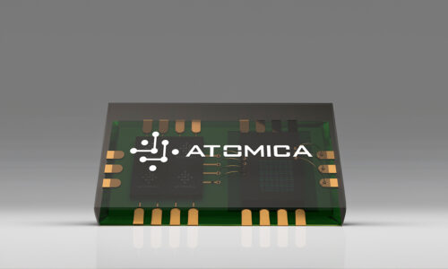
Atomica’s pioneering TSV technology provides advanced applications today and sets the foundation for future interconnection architecture. With a strong history in MEMS, Atomica has the technical and economic flexibility to halve the iterative time for TSV design, prototyping, and validation, staying years ahead of competitors.
Great Value in TSV Technology
TSVs are vertical electrical connections passing through silicon wafers or chips, enabling compact, multi-layer packages. Despite their simple concept, the application of TSVs is complex yet transformative, allowing for smaller footprints, shorter signal paths, and increased integration. TSVs are critical for 2.5D and 3D IC integrations, with future trends pointing towards heterogeneous 3D integration and the co-packaging of electronic circuits and MEMS. TSV-enabled layers allow the combination of different materials and devices into a single package, something unachievable on a single CMOS wafer.
Today, TSVs enable advanced semiconductor assembly with tightly packed dies and stacked IC layers. In 2.5D integration, multiple chips are placed side-by-side on an interposer, which aids heat dissipation and provides efficient TSV interconnects, commonly used in high-performance computing and consumer electronics. 3D homogeneous integration involves vertically stacked IC dies interconnected through TSVs, enhancing power efficiency and communication paths but introducing thermal considerations due to increased component density. These 3D ICs are used in applications requiring high integration levels, like high-bandwidth memory and specialized processors.
Here Comes the Future
The push for more functionality in smaller spaces leads to new packaging complexities. 3D heterogeneous IC integration allows the stacking of diverse dies with different functionalities, technologies, and manufacturing processes, expanding overall package capabilities. This approach combines logic circuits, memory, power management, and communication interfaces, tailored to specific functions for more efficient operation. By combining multiple functionalities in a single package, heterogeneous integration reduces the need for additional components, connectors, and interconnects, leading to cost savings in materials, assembly, and testing.
Another emerging development is the co-packaging of electronic circuits with MEMS for applications like wearable devices, implantable medical devices, and aerospace microelectronics. Integrating CMOS ICs with MEMS requires careful consideration of material compatibility, processing steps, and design methodologies to prevent stress-induced damage or performance degradation.
Despite challenges, this integration offers significant benefits, including enhanced functionality, improved performance, and reduced system footprint. TSVs will continue to be crucial in minimizing footprints and optimizing performance through component stacking.

Customization and Standardization – Both Through TSVs
TSVs are essential in both 2.5D and 3D packages, implemented through customization or standardization. Customization optimizes performance for specific applications, though it incurs higher costs and longer development times due to the intricate design, prototyping, and validation processes involved. Standardization offers streamlined, cost-effective solutions, reducing time to market by using pre-designed TSV interposers. This approach is advantageous for mass production, benefiting from economies of scale and shorter lead times.
Customized TSVs:
| Pros | Cons |
|
|
|
|
|
Standardized TSV Interposers:
| Pros | Cons |
|
|
|
|
|
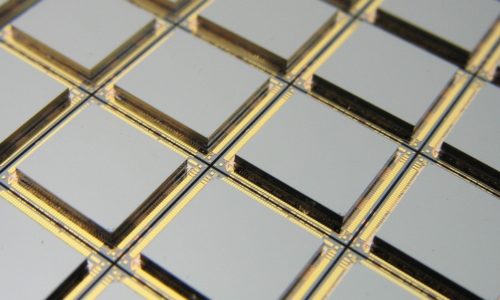
Atomica meets diverse customer needs with both standard and customized TSV solutions. Offering standard interposer platforms with TSV diameters ranging from 10 to 60 micrometers and a minimum pitch of twice the diameter, Atomica also excels in designing custom TSVs and interposers tailored to specific requirements. This includes variations in silicon substrate thickness, TSV diameter, pitch, and aspect ratio. Additionally, Atomica can apply electrochemically plated redistribution layers (RDLs) on the interposer surfaces to form additional interconnects with the TSVs, enhancing integration capabilities.
Considerations in TSV Design
The thermal budget for the package – the maximum allowable temperature range during the fabrication and operation of the device – significantly impacts TSV design and implementation.
Regardless of size, spacing, or location, all TSVs follow the same basic steps:
- Hole Creation: Using deep reactive ion etching, a hole is created in the silicon substrate, alternating etching with a polymer passivation coating to control lateral expansion until the desired depth is reached.
- Dielectric Layer Deposition: A dielectric layer is deposited on the internal surface of the via to prevent signal loss into the substrate.
- Barrier/Seed Layer Deposition: A conductive barrier/seed layer is deposited to prime the cavity.
- Via Filling: The via is filled with a conductive material, commonly copper, using electrochemical deposition.
- Polishing: The via fill and seed layer are chemically-mechanically polished (CMP) from the front side to expose the filled TSV.
- Backside Polishing: The backside of the wafer is polished to expose the bottom of the filled via.
- Pad Placement: Bonding and landing pads are placed at the top and bottom of the filled via for electrical connections.
Heat application during etching and deposition processes can challenge the thermal budget, depending on the timing of TSV fabrication, which can be categorized into via first, via middle, and via last.
- Via-First: TSVs are fabricated early, before active device layers are built, avoiding thermal stress on functional circuitry and allowing efficient heat dissipation.
- Via-Middle: TSVs are built after active device layers but before back-end-of-line (BEOL) metallization, minimizing thermal stress while ensuring proper TSV formation, and improving signal integrity by placing TSVs close to active devices.
- Via-Last: TSVs are inserted after active device layers and BEOL metallization, requiring careful management to avoid damage to completed structures, and simplifying overall manufacturing through tight integration.
Why Atomica?
Atomica has the cutting-edge tools, sophisticated manufacturing processes, and expertise to create high-quality TSVs, microscopic MEMS, and advanced integrated packages. With deep experience in material science, Atomica offers a wide array of plating materials, including copper (Cu), gold (Au), silver (Ag), indium (In), nickel (Ni), tin (Sn), and alloys such as iron-nickel (NiFe) and gold-tin (AuSn). Atomica’s outstanding capabilities in bonding techniques, including thermal compression, fusion, direct bonding, polymer bonding, and hybrid bonding, enable unique solutions like bonding stacks of four silicon wafers.
The company’s early learning efforts have paved the way for future efficiency in wafer-scale heterogeneous 3D IC platforms with full control, monitoring, and communication functionality. Ultimately, Atomica’s proven track record of combining tools, processes, and experience makes it the ideal partner to meet customers’ most challenging needs, ensuring high-quality, reliable products designed to meet the demands of modern semiconductor applications.