
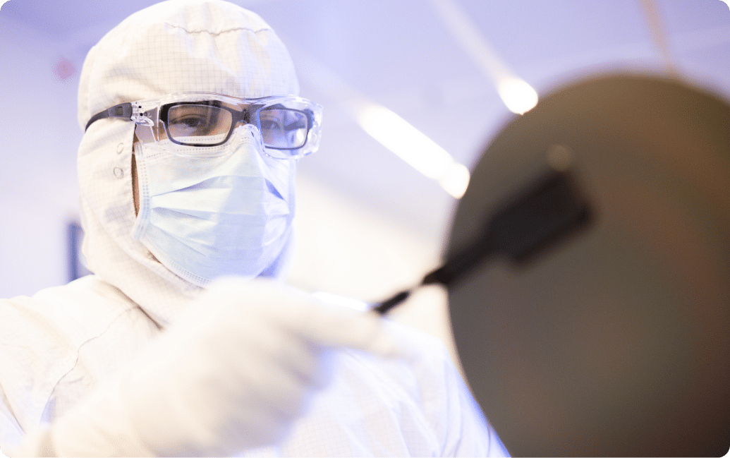
- Chemical Mechanical Polishing (CMP) CMP is a process that combines chemical and mechanical forces to planarize the surface of a wafer, removing excess material and achieving a smooth, flat surface. This is done using an abrasive slurry and polishing pad.
- Etch-Back Planarization Etch-back planarization involves selectively etching back materials (such as oxides or polymers) to achieve surface uniformity. This technique is commonly used to level surfaces by removing uneven layers.
- Electrochemical Planarization Electrochemical planarization is a technique where a wafer’s surface is planarized using electrochemical reactions to selectively remove material. This is typically done with a combination of electric current and chemical etching solutions.
- Wafer Grinding Wafer grinding is a back-thinning process where the backside of a wafer is ground to reduce its thickness, making it suitable for specific applications such as flexible electronics or devices requiring ultra-thin wafers.
- Wafer Polishing Wafer polishing is the process of refining the surface of a wafer to achieve a smooth, defect-free surface with low roughness. This is typically done using a combination of mechanical polishing and chemical treatments.
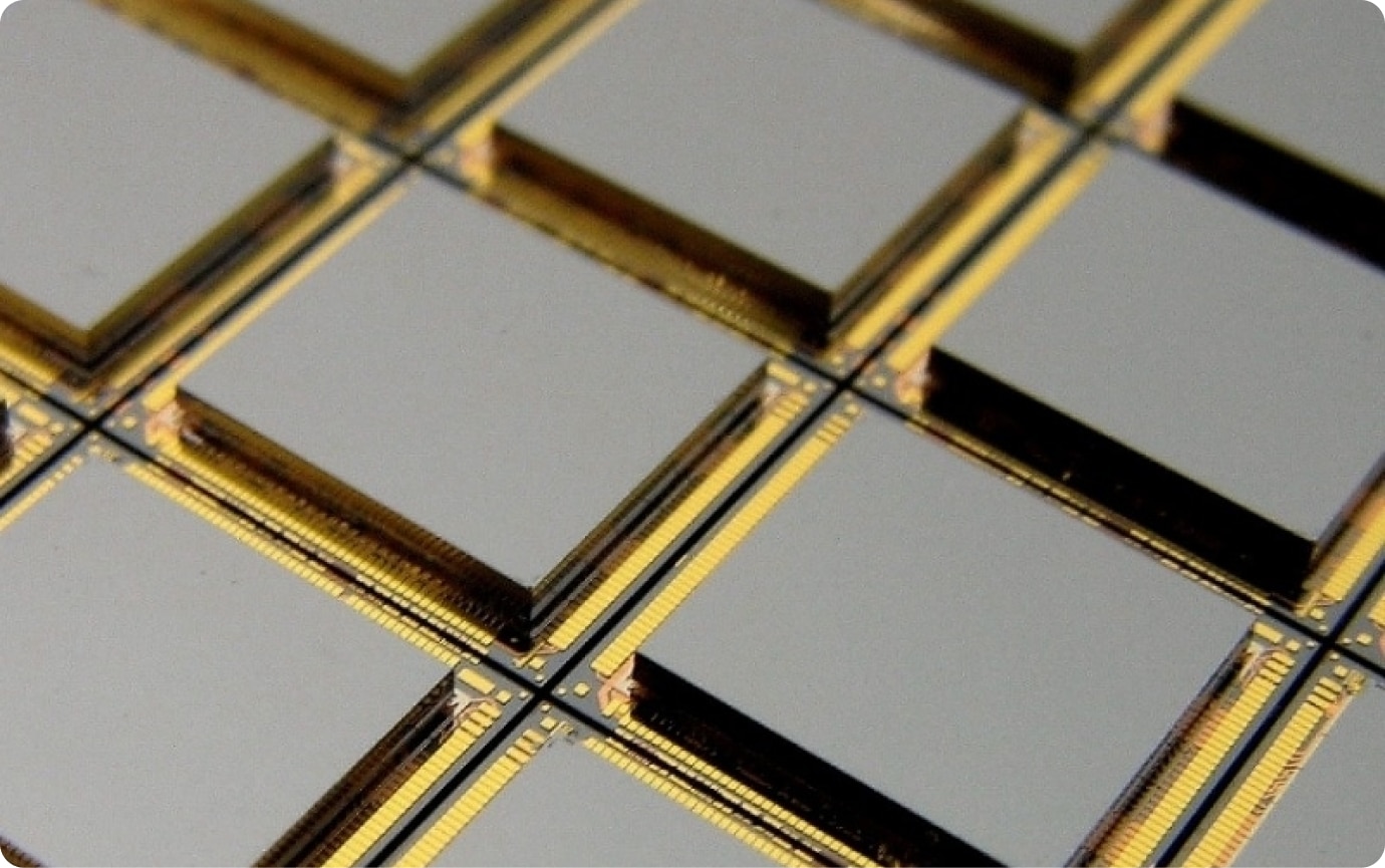
- Wafer Dicing Wafer dicing is the process of cutting a silicon wafer into individual semiconductor chips or dies. This is typically done using a diamond-tipped saw blade or laser dicing tools, allowing precise cutting along pre-defined scribe lines.
- Wafer Dicing Pad Reveal Wafer dicing pad reveal refers to the process of exposing specific areas, such as bond pads, by removing surrounding materials or protective layers during or after the dicing process. This ensures the pads are accessible for bonding or wire connection.
- Wafer Dicing Scrub Wafer dicing scrub is a post-dicing cleaning process used to remove particles, contaminants, or residual material left on the wafer after dicing. This process ensures that the dies are clean and ready for packaging.
For more details on our back end capabilities, please contact our technical team or download our fab technology guide.
Other Capabilities

Why Atomica?
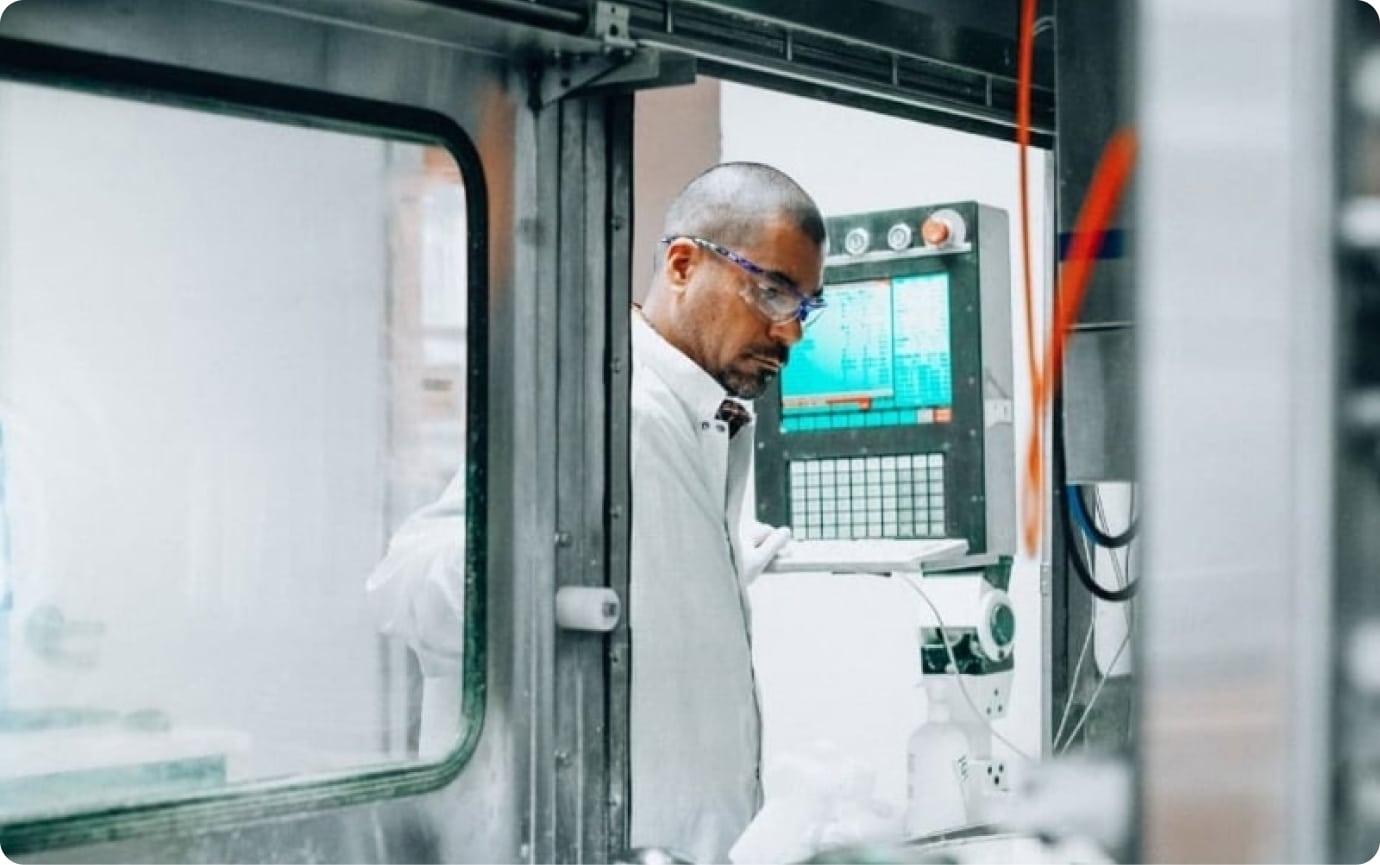
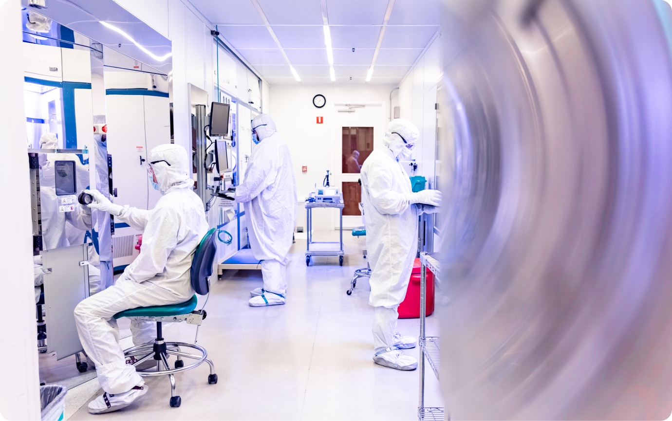
Atomica focuses on the success of our customers’ products, with rapid prototyping and scalable production. We are a leader in microfabrication, including photonics, sensors, biotechnology, and MEMS. We provide customers device optimization, faster speed to market, and cost-efficient fabrication. Atomica operates a 30,000-square-foot class 100 cleanroom near Santa Barbara, California, supporting a wide range of capabilities and materials with ISO 9001 certification and ITAR registration. We leverage sophisticated process control analytics, artificial intelligence inspection, advanced metrology, and proprietary fab operations systems to maximize efficiency.

Next Steps
Learn how Atomica created the world’s most sophisticated MEMS device.
Talk to our engineering team about your backend processing needs.
Master Deep RIE: Atomica’s Expertise, Techniques and Tool Set in DRIE.