Atomica offers the ability to adapt our tests to fit our customers’ specific application needs. The immediate feedback reduces development time and improves process optimization. Ultimately, this leads to faster time to market and higher yield.
Testing is a critical component of microfabrication, including MEMS, sensors, photonics, and biochips, ensuring device performance, reliability, and quality. Given the complexity of these devices, comprehensive testing helps identify and eliminate defects early, reducing costs and improving yield. Atomica’s in-process electrical testing includes measurements of capacitance, resistance, inductance, and isolation, enabling real-time verification of functionality. For unique applications, we also provide custom testing solutions tailored to meet specific customer requirements, ensuring that only high-quality, known-good dies are delivered, optimizing production efficiency and device reliability.
- Electrical Testing Electrical testing in microfabrication is used to evaluate the electrical properties of microelectronic devices and materials, including conductivity, resistivity, capacitance, and device performance characteristics. This testing ensures that the devices meet design specifications and function correctly.
- Mechanical Testing Mechanical testing in microfabrication assesses the mechanical properties of materials and devices at micro and nanoscale. This includes measuring hardness, elasticity, tensile strength, adhesion, and fracture toughness. Various techniques like nanoindentation, tensile testing, and bending tests are employed.
- Thermal Testing Thermal testing examines how materials and devices behave under different temperature conditions, focusing on properties like thermal conductivity, thermal expansion, and heat dissipation. It ensures that devices can operate reliably across a range of temperatures.
For more details on our testing capabilities, please contact our technical team or download our fab technology guide.
Other Capabilities
Why Atomica?
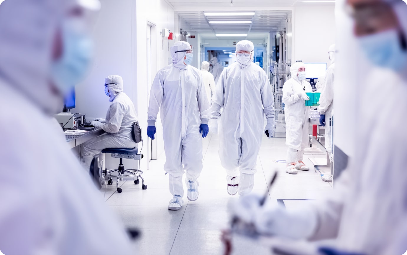
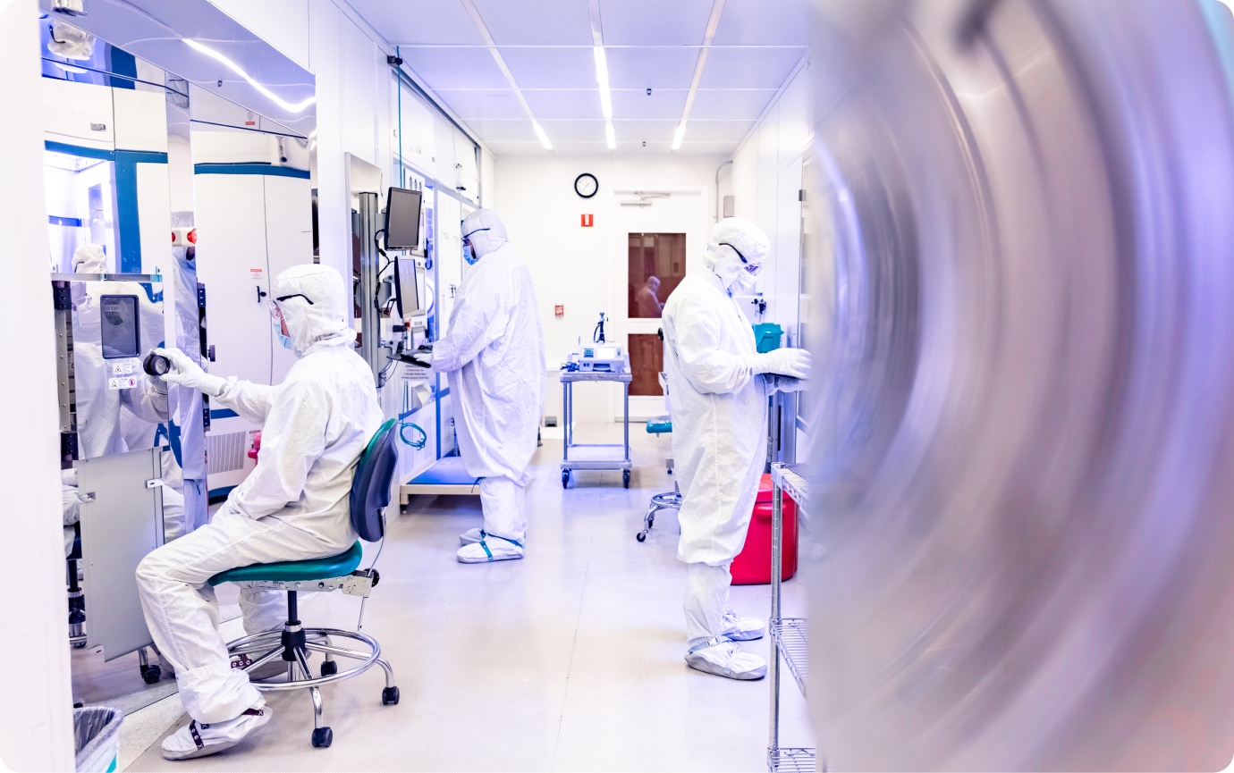
Atomica focuses on the success of our customers’ products, with rapid prototyping and scalable production. We are a leader in microfabrication, including photonics, sensors, biotechnology, and MEMS. We provide customers device optimization, faster speed to market, and cost-efficient fabrication. Atomica operates a 30,000-square-foot class 100 cleanroom near Santa Barbara, California, supporting a wide range of capabilities and materials with ISO 9001 certification and ITAR registration. We leverage sophisticated process control analytics, artificial intelligence inspection, advanced metrology, and proprietary fab operations systems to maximize efficiency.


Next Steps

See how we created the world’s most sophisticated MEMS device.

Talk to our engineering team about your project.

Read about our investment in cutting-edge MEMS tools
