Atomica’s Dry Etch capabilities
Atomica offers various dry etching capabilities. Specifically, our Deep reactive ion etching (DRIE) capability allows anisotropic etching of silicon which is useful for etching of close-tolerance comb fingers, vias or holes, and trenches. Read more of offering below.
- Plasma Etch Plasma etching is a dry etching technique that uses plasma to remove material from a substrate. A gas (such as oxygen or a halogen compound) is ionized into plasma, and reactive ions or radicals chemically react with the material to etch it away. Plasma etching provides isotropic or anisotropic etching based on the process conditions.
- Inductively Coupled Plasma (ICP) Etch ICP etching uses a high-density plasma generated by inductively coupling energy into the chamber. This method produces a high concentration of reactive ions, resulting in precise, anisotropic etching while allowing for independent control of ion density and energy.
- Reactive Ion Etch (RIE) RIE is a dry etching process where reactive ions are accelerated toward the substrate to remove material. It allows for both chemical and physical etching components and provides fine control over feature size and depth.
- Deep Reactive Ion Etch (DRIE) Deep Reactive Ion Etch (DRIE) is an advanced etching technique used in microfabrication to create deep, high-aspect-ratio features in substrates like silicon. It uses alternating cycles of plasma etching and passivation to achieve nearly vertical sidewalls with minimal undercutting. DRIE operates in two steps: an etch phase using reactive ions (typically SF6) to remove material from the substrate, followed by a passivation phase using a polymerizing gas (usually C4F8) to coat the sidewalls and protect them from lateral etching. This cycle is repeated multiple times to achieve deep etch depths with high anisotropy (sharp, vertical sidewalls).
- Ion Beam Etch (IBE) IBE uses a focused beam of ions to physically etch away material from the surface of a substrate. Unlike chemical etching, it relies solely on the physical bombardment of ions and is highly directional.
- O2 Resist Strip O2 resist stripping uses oxygen plasma to remove photoresist from the surface of a substrate. The oxygen ions react with the organic components of the resist, turning them into volatile compounds that can be pumped away.
- O2 Descum O2 descumming is a process that uses oxygen plasma to remove a very thin layer of residual resist or organic contaminants after photolithography, usually before etching or deposition steps.
For more details on our etching capabilities, please contact our technical team or download our fab technology guide.
Other Capabilities
Why Atomica?
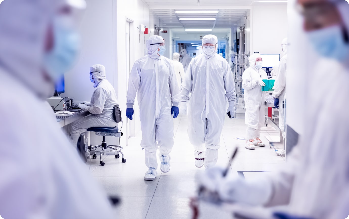
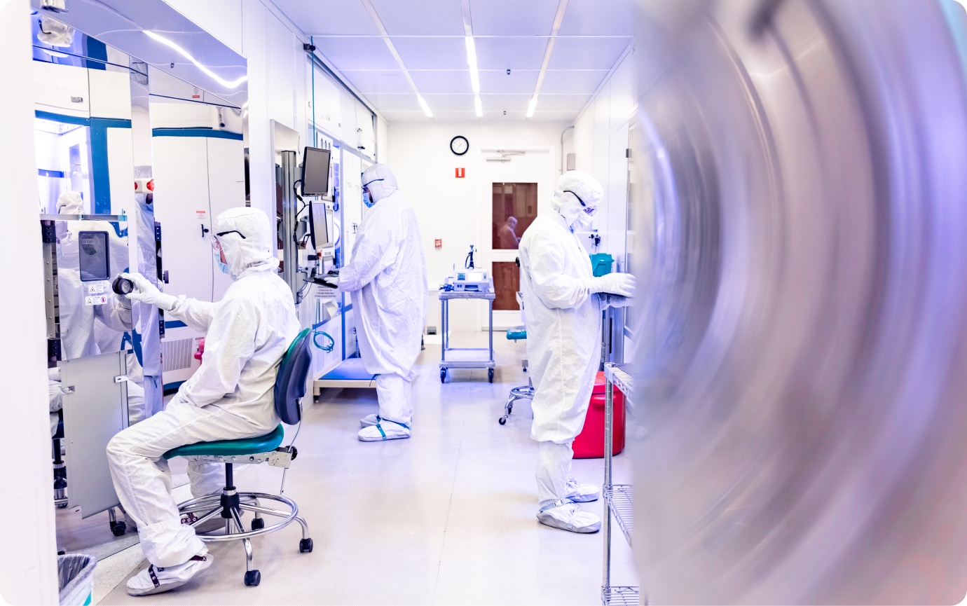
Atomica focuses on the success of our customers’ products, with rapid prototyping and scalable production. We are a leader in microfabrication, including photonics, sensors, biotechnology, and MEMS. We provide customers device optimization, faster speed to market, and cost-efficient fabrication. Atomica operates a 30,000-square-foot class 100 cleanroom near Santa Barbara, California, supporting a wide range of capabilities and materials with ISO 9001 certification and ITAR registration. We leverage sophisticated process control analytics, artificial intelligence inspection, advanced metrology, and proprietary fab operations systems to maximize efficiency.


Next Steps

Master Deep RIE: Atomica’s Expertise, Techniques and Tool Set in DRIE

Talk to our engineering team about your Dry Etching project

Learn more about Atomica’s Omega Rapier Plasma Etch Capabilities