Moving optical connectivity closer to compute

PRESS RELEASE
Atomica Launches AI Optical Connectivity Platform to Address the Physical Bottleneck in AI Infrastructure
SANTA BARBARA, CA, June 30, 2026 (PRNewswire-PRWeb)
Atomica’s AI Optical Connectivity Platform addresses a growing physical bottleneck in AI infrastructure: the need to move more data with greater bandwidth, lower latency, and lower power. The platform helps customers build the microfabricated alignment, packaging, and integration structures required for optical connectivity in next-generation AI systems.
Atomica, a U.S.-based microfabrication foundry, today announced the launch of its AI Optical Connectivity Platform, a new microfabrication platform for companies building the optical, mechanical, thermal, and packaging structures required to scale next-generation AI infrastructure.
The next era of AI will not be unlocked by processors alone. As AI clusters grow larger, denser, and more power-hungry, the industry is running into a physical reality: moving data is becoming as critical as processing data.
Electrical interconnect will remain essential, but it is no longer enough on its own. The growth of AI requires higher bandwidth, lower power, shorter electrical paths, tighter integration, better thermal control, and more scalable packaging. That shift is pushing optical connectivity closer to GPUs, accelerators, switches, memory systems, and compute packages.
"AI is forcing the hardware industry to rethink the physical layer. The challenge is no longer just processor speed. It is moving data efficiently across thousands of processors without wasting power, space, or thermal budget. Optical connectivity is becoming one of the most important answers, and Atomica is focused on making these systems manufacturable.

— Eldon Klaassen, CEO of Atomica
Atomica’s AI Optical Connectivity Platform is designed for this transition. The platform supports precision fiber alignment, silicon optical benches, V-grooves, microlenses, micromirrors, waveguide structures, optical alignment features, wafer-level packaging elements, interposers, TSV and TGV integration structures, optical engine packaging components, and thermal management microstructures.
As optics move closer to compute, the challenge becomes more than optical performance alone. Photonic chips, lasers, fiber arrays, and optical engines all depend on a precision integration layer that can align, route, package, protect, cool, and connect optical components inside real hardware. Small variations in placement, thermal drift, package stress, or coupling efficiency can become major system-level constraints when multiplied across thousands of optical channels.
Atomica’s platform brings together established process capabilities, design modules, materials knowledge, and integration methods that can be adapted to customer-specific optical connectivity architectures. This gives customers a more structured technical foundation for the critical alignment, packaging, optical, mechanical, thermal, and integration elements required to move from photonic innovation to manufacturable hardware.
The platform is designed for companies developing optical transceivers, silicon photonics packages, fiber array units, optical engines, external laser source modules, near-packaged optics, co-packaged optics, TFLN-based optical systems, optical MEMS devices, LiDAR systems, photonic sensors, and compact optical systems that require precise alignment and integration.
“Many companies can demonstrate optical innovation in the lab,” Klaassen added. “The harder question is whether those systems can be aligned, packaged, tested, cooled, and manufactured repeatably. That is the gap Atomica is built to help close.”
The launch is part of Atomica’s broader strategy to support the physical infrastructure of AI hardware, including optical source integration, photonic packaging, thermal microstructures, physical AI sensors, MEMS optical control systems, and biotechnology microdevices. Atomica’s view is that the future of AI hardware will depend not only on faster chips, but on the physical technologies that connect, cool, sense, package, and integrate advanced systems.

About Atomica
Atomica is a U.S.-based microfabrication foundry that builds advanced platforms for AI hardware, photonics, sensors, MEMS, and biotechnology devices.
Atomica supports customers developing AI optical connectivity, AI optical source integration, AI photonic packaging, AI thermal microstructures, physical AI sensors, MEMS optical control systems, and biotechnology microdevices with rapid prototyping and scalable production.
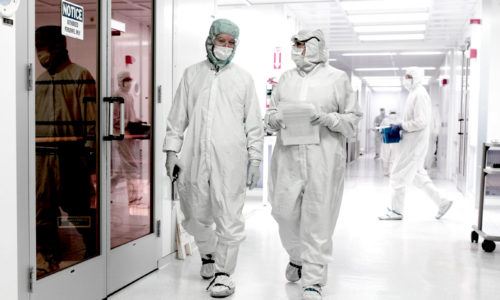
Atomica operates a 30,000-square-foot Class 100 cleanroom near Santa Barbara, California, supporting a wide range of capabilities and materials with ISO 9001 certification and ITAR registration. Capabilities include photolithography, deposition, dry etch, wet etch, bonding, plating, metrology, testing, dicing, and planarization. Atomica leverages engineering collaboration, process standardization, modeling and simulation, artificial intelligence optimization, and proprietary fab technology to achieve customer objectives.