Atomica’s diverse metrology tools, enhanced with AI analysis, deliver precise, data-driven insights for optimizing MEMS, sensors, photonics, and biotech device performance and manufacturing efficiency.
Atomica’s advanced metrology capabilities integrated with AI-driven analysis, provide unparalleled precision and efficiency for microfabrication, including MEMS, sensors, photonics, and biochips. These tools ensure accurate measurement of critical dimensions, film thickness, and surface properties, guaranteeing devices meet exact specifications. AI enhances this process by analyzing data in real time, identifying trends, and predicting issues before they impact yield. This proactive approach improves process control, accelerates development cycles, and optimizes material usage, helping customers deliver reliable, high-performance devices while reducing costs.
- Scanning Electron Microscopy (SEM) SEM is a type of electron microscope that uses focused beams of electrons to scan the surface of a sample. The electrons interact with the sample’s atoms, producing signals that provide information about the sample’s surface topography, composition, and morphology.
- Focused Ion Beam (FIB) Analysis FIB uses a beam of focused ions, typically gallium, to mill or sputter material from a surface at a nanoscale. It can also be used to image or modify surfaces, including cross-sectioning for further analysis.
- Energy Dispersive X-ray Spectroscopy (EDS) EDS is an analytical technique used with electron microscopy that detects X-rays emitted from a sample when it is hit by a high-energy beam of electrons. These X-rays provide elemental composition information.
- Atomic Force Microscopy (AFM) AFM is a high-resolution imaging technique that uses a sharp probe (cantilever) to scan the surface of a sample. It measures topography at the nanoscale by recording the deflection of the probe due to interactions with the surface.
- Ellipsometry Ellipsometry is an optical technique for measuring thin film thickness and refractive index. It works by analyzing the change in polarization of light reflected from the surface.
- Microscopy Microscopy encompasses techniques used to magnify small objects or features, making them visible to the human eye or a camera. Techniques include optical, electron, and scanning probe microscopy.28
- Confocal Microscopy Confocal microscopy is an optical imaging technique that uses a spatial pinhole to eliminate out-of-focus light, improving image resolution and depth. It provides 3D imaging of samples.
- Sheet Resistance Sheet resistance is a measure of resistance for thin films of uniform thickness. It is defined as the resistance across a square area of the film and is expressed in ohms per square.
- Contact Angle Analyzer A contact angle analyzer measures the angle formed between a liquid droplet and a solid surface, which helps determine surface wettability and energy.
- Profilometry Profilometry is a technique used to measure the surface profile of a material, including its roughness and texture. It can be contact-based or optical.
- X-ray Fluorescence Spectroscopy (XRF) XRF is a non-destructive analytical technique that uses X-ray irradiation to excite atoms in a sample, causing them to emit secondary (fluorescent) X-rays that reveal the sample’s elemental composition.
- Front to Back Alignment Check Front to back alignment checks involve aligning the front and back patterns of a wafer during photolithography, ensuring that the structures on both sides are properly aligned. 29
- IVS Metrology IVS (Integrated Virtual Metrology System) metrology refers to real-time, in-line measurement and control of process parameters, often used in conjunction with semiconductor fabrication tools.
- Image Capture & CD Measurement Image capture in microfabrication refers to the use of cameras, microscopes, or imaging systems to visually document the surface, structure, or features of a fabricated device. High-resolution images help assess defects, material quality, and pattern fidelity.
- Spectroscopic Reflectometry Spectroscopic reflectometry is a non-destructive optical technique used to measure the thickness and optical properties of thin films. It involves shining light of varying wavelengths onto a film and measuring the reflected light’s intensity as a function of wavelength. By analyzing the interference patterns created by the reflections from the different film interfaces, the thickness and refractive index of the film can be determined.
For more details on our metrology capabilities, please contact our technical team or download our fab technology guide.
Other Capabilities
Why Atomica?
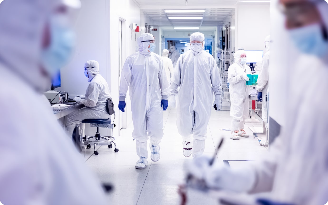
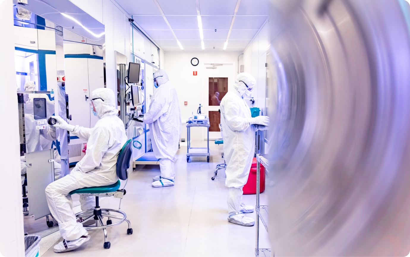
Atomica focuses on the success of our customers’ products, with rapid prototyping and scalable production. We are a leader in microfabrication, including photonics, sensors, biotechnology, and MEMS. We provide customers device optimization, faster speed to market, and cost-efficient fabrication. Atomica operates a 30,000-square-foot class 100 cleanroom near Santa Barbara, California, supporting a wide range of capabilities and materials with ISO 9001 certification and ITAR registration. We leverage sophisticated process control analytics, artificial intelligence inspection, advanced metrology, and proprietary fab operations systems to maximize efficiency.


Next Steps

See how we created the world’s most sophisticated MEMS device.

Talk to our engineering team about your project.

Read about our investment in cutting-edge MEMS tools