-
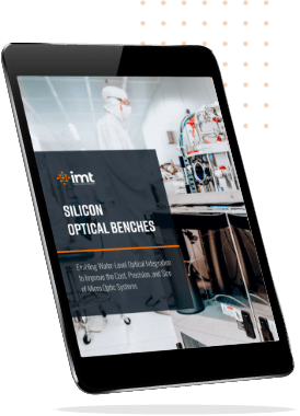
Silicon optical benches (SiOBs)
Atomica’s silicon optical benches (SiOBs) enable highly integrated optical engines and laser packaging at the wafer level without requiring active alignment. Our SiOBs also underlie radio frequency (RF) photonics and RF over fiber. SiOB-based integration of components onto a device improves the economics of wafer-level processing and testing, and hermetic packaging improves your device’s lifetime. Read more.
-
Through Silicon Vias (TSVs)
Through Silicon Vias (TSVs) allow electrical signals to pass through substrates, yielding smaller device sizes and a reduced signal path. Thanks to our decades of experience with TSVs, Atomica is manufacturing products today with nearly 140,000 hermetic metal-filled TSVs per wafer. Atomica’s customers use TSVs to reduce routing complexity and increase integration while maintaining – or in some cases shrinking – the device’s footprint. Read more.
-
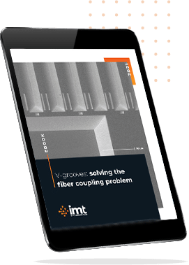
V-grooves
Our unique V-groove processing capabilities deliver high-precision coupling of fibers into a photonic circuit. High coupling efficiency and minimizing the need for active alignment deliver cost advantages and smaller device footprints for Atomica’s customers. Read more.
-
MEMS mirrors
By steering light, MEMS mirrors are the critical foundation for AR/VR, variable optical attenuators (VOA), and more. Our 20+ years of experience fabricating all manner of MEMS mirrors empowers us to help commercialize your product. Read more.
-
Fiber management blocks
Our expertise with fiber block fabrication positions us to produce precise fiber management structures for dense, small optical systems.
-
CMOS post-processing
Atomica brings a suite of post-processing technologies that are crucial for adding features and structures at the wafer level, particularly materials and structures not available in a CMOS fab, such as cavities, fiber coupling structures, laser submounts, wafer bonding, and gold deposition.
-
Laser submounts
Atomica’s laser submounts facilitate 3D placement of lasers with much higher precision than traditional ceramic submounts.
-
Gold Tin (AuSn)
Gold-tin metallurgy is critical for attaching lasers to photonic systems. Atomica offers the rare capability of AuSn deposition, which is not accessible with a traditional CMOS fab.
-
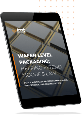
Wafer-level packaging
Our hermetic packaging protects laser facets from degradation, extending the lifetime of our customers’ devices. Read more.
-
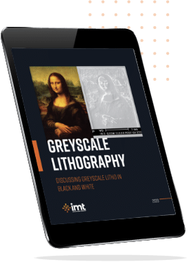
Greyscale (3D) lithography
Patterning features on a wafer through lithography is a fundamental building block in creating MEMS components and devices. Atomica offers a suite of tools and process capabilities to deliver lithography that is highly precise and highly repeatable. In particular, our advanced greyscale (3D) lithography capabilities produce high-density microlens arrays to direct light. Read more.
-
Photonic circuits and waveguides
Atomica has 20+ years of experience and capabilities for fabricating custom waveguides and photonic circuits. Holographic waveguides for creating visual images with red, green, and blue light sent through the waveguide are an exciting area of innovation that Atomica is proud to support.