Wafer Level Packaging (WLP)
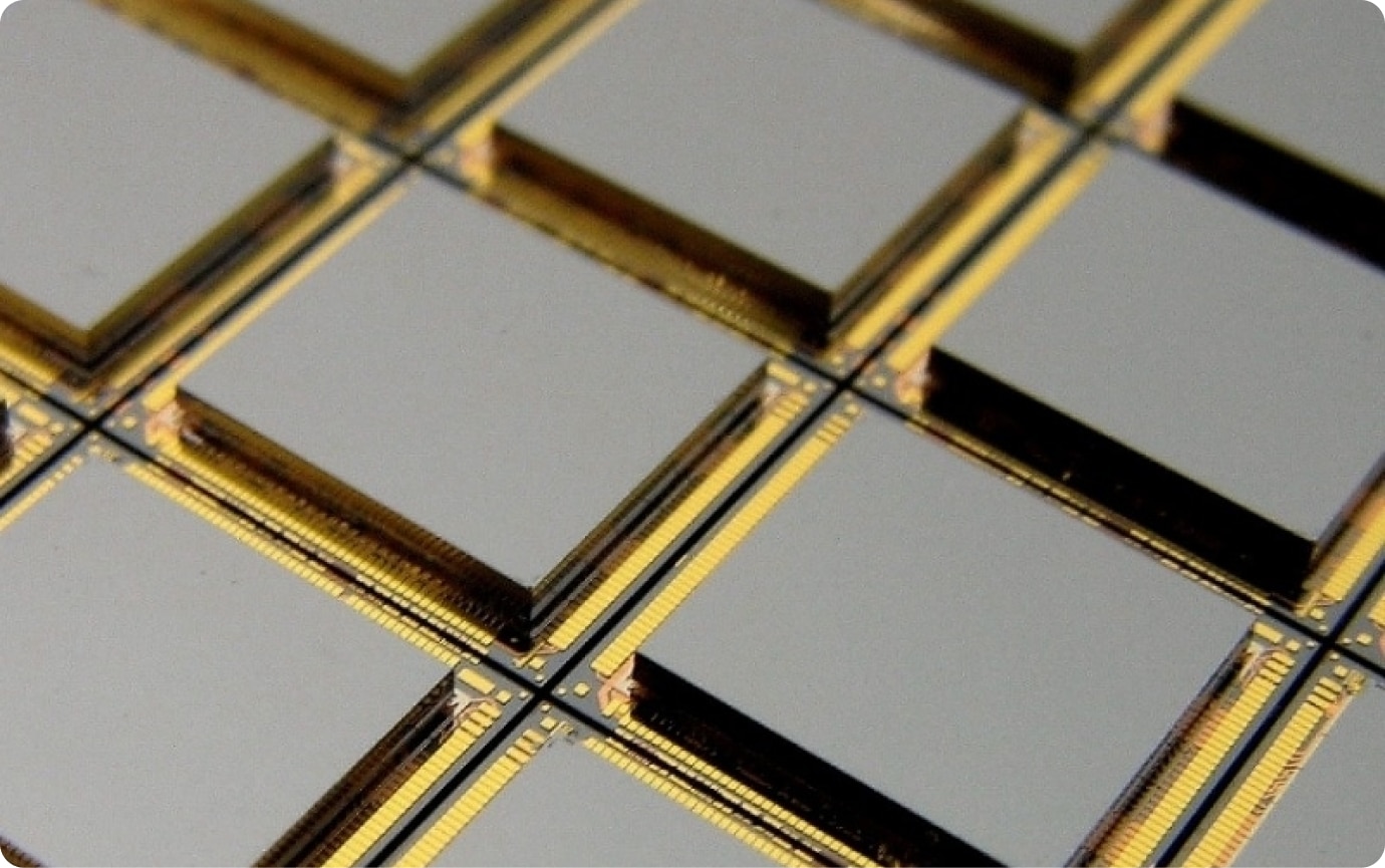
More than 80% of programs at Atomica implement wafer level packaging (WLP) with some projects requiring as many 6 wafers for integration and miniaturization.


Other Capabilities
Why Atomica?
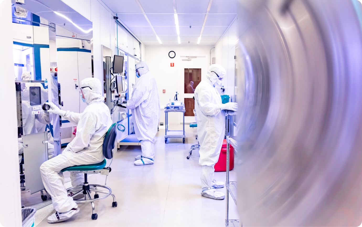
Atomica focuses on the success of our customers’ products, with rapid prototyping and scalable production. We are a leader in microfabrication, including photonics, sensors, biotechnology, and MEMS. We provide customers device optimization, faster speed to market, and cost-efficient fabrication. Atomica operates a 30,000-square-foot class 100 cleanroom near Santa Barbara, California, supporting a wide range of capabilities and materials with ISO 9001 certification and ITAR registration. We leverage sophisticated process control analytics, artificial intelligence inspection, advanced metrology, and proprietary fab operations systems to maximize efficiency.

Next Steps

Learn Wafer Bonding techniques and the importance for MEMS

Talk to our engineering team about your WLP project

Download our comprehensive eBook on Wafer Level Packaging