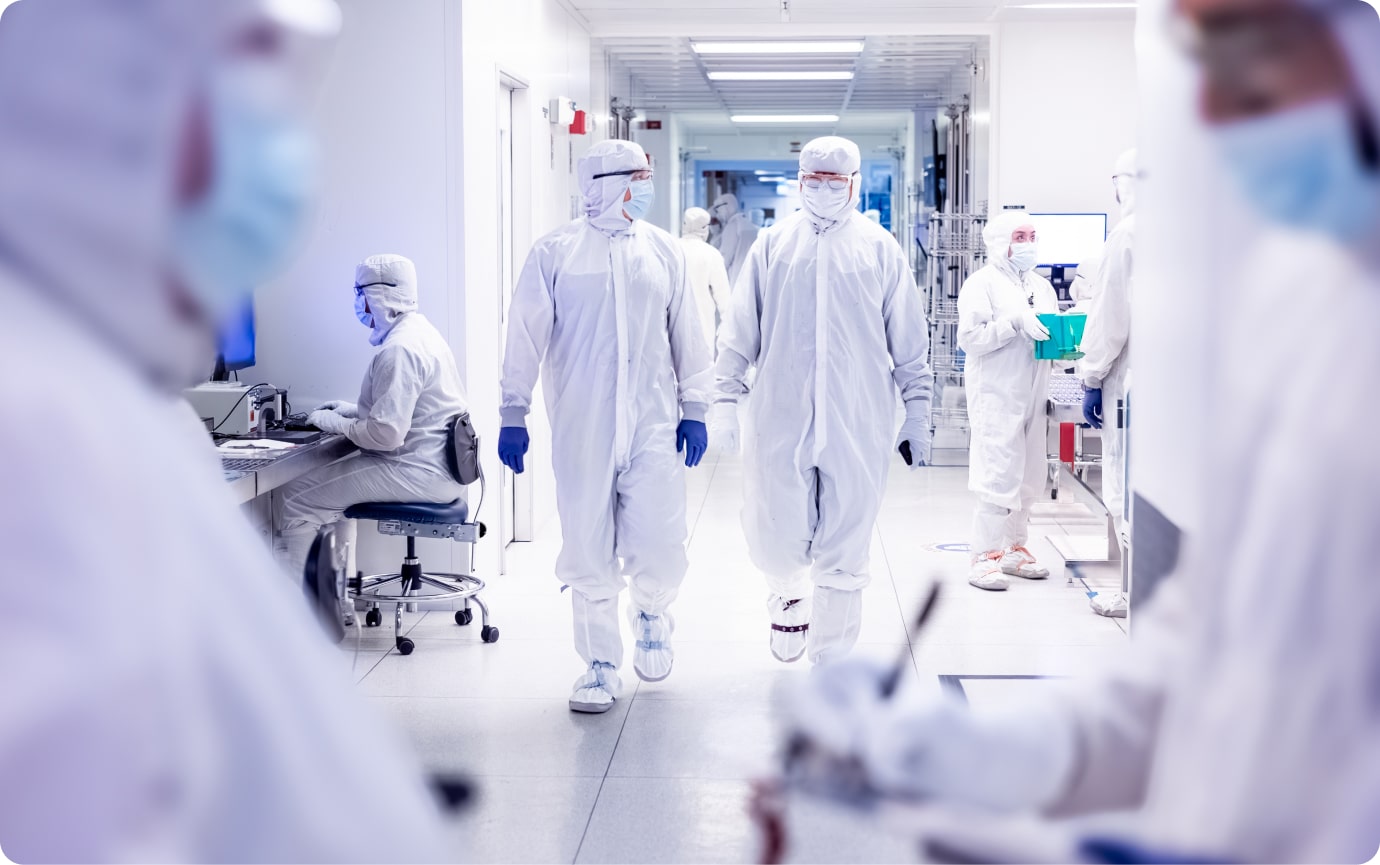
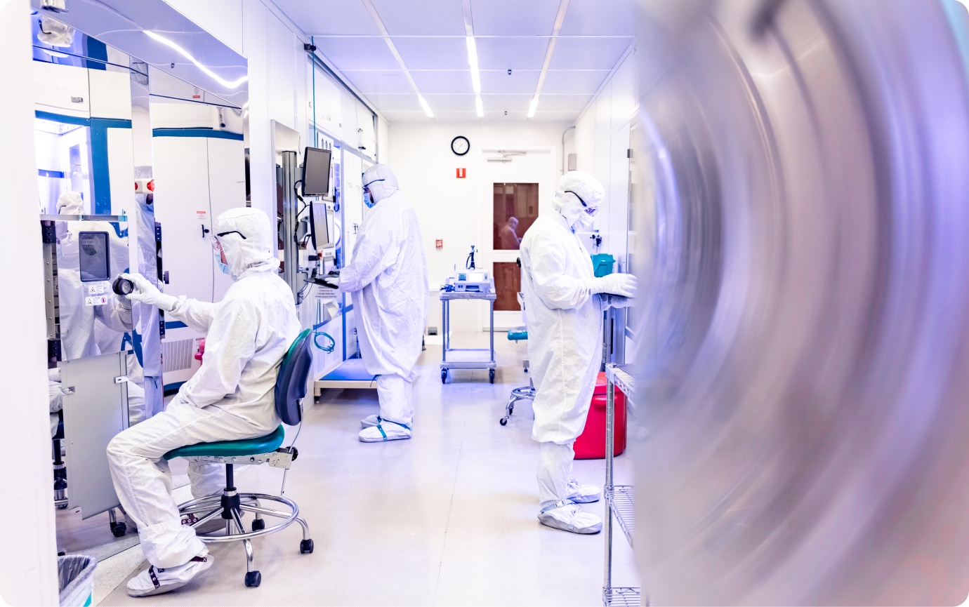
Atomica delivers precision and repeatability in photolithography through the use of advanced automated steppers. These systems achieve highly accurate layer-to-layer alignment and resolve submicron features with ease. Automation ensures error-free exposure, enabling consistent, repeatable processes that support high-volume production with exceptional quality.


Atomica’s photolithographic capabilities
Tight CD and overlay controls are critical to building complex photonics, sensors, biotech and MEMS. Many programs require 15 to 20 mask layers, some > 30. Atomica offers the following capabilities:
- Projection Lithography (Steppers/Scanners) Projection litho uses lenses to project a reduced image of the mask onto the wafer, allowing high precision without direct contact. Widely used in semiconductor and MEMS manufacturing for its scalability and precision.
- I-Line Lithography I-Line lithography is a photolithography technique that uses a 365 nm wavelength UV light source (i-line of mercury) to pattern features on a substrate. It is widely used in microfabrication for devices with feature sizes in the submicron range.
- Contact Lithography Contact lithography involves directly placing a photomask in physical contact with a photosensitive material (photoresist) on a substrate during exposure to UV light. The resolution is limited by the quality of contact between the mask and resist.
- Proximity Lithography Proximity lithography is similar to contact lithography but with a small gap between the mask and the substrate, reducing mechanical damage but slightly lowering resolution compared to contact lithography.
- Phase-Shift Mask (PSM) Lithography PSM lithography uses masks that introduce a phase shift in the light passing through specific regions, enhancing the resolution of features by improving the contrast between light and dark areas.
- Multi-patterning Lithography Multi-patterning lithography involves multiple exposure and etching steps to achieve feature sizes smaller than the wavelength of light used in the lithographic process. It includes techniques such as double or quadruple patterning.
- Greyscale Lithography Greyscale lithography is a technique that creates 3D structures with varying heights by modulating the intensity of the light used to expose the photoresist, resulting in varying depths of exposure.
- Polymer Lithography Polymer lithography refers to the use of polymer-based materials in the lithography process, either as resists or as the substrate material itself, to pattern structures on micro- and nanoscale.
- Bi-Layer LOR/Resist Bi-layer lithography uses two layers: an LOR (Lift-Off Resist) layer and a photoresist layer. The LOR creates an undercut beneath the photoresist, aiding in clean liftoff during metal deposition.
- Positive Photoresist In positive photoresist, the exposed regions become soluble in the developer solution, allowing those areas to be removed, while the unexposed regions remain intact.
- Negative Photoresist Negative photoresist works oppositely to positive resist: the exposed regions harden and remain after development, while the unexposed regions are removed.
- Dry Film Resists Dry film resists are pre-coated photoresist films that are laminated onto substrates. They are typically used for applications requiring fast processing and uniform thickness across large areas.
Shadow Masking:
For less precision metal deposition, shadow masking can also be used for depositing metals or metal stacks. Atomica can make higher precision silicon shadow masks or stainless steel shadow masks.
For more details on our plating capabilities, please contact our technical team or download our fab technology guide.
Other Capabilities
Why Atomica?
Atomica focuses on the success of our customers’ products, with rapid prototyping and scalable production. We are a leader in microfabrication, including photonics, sensors, biotechnology, and MEMS. We provide customers device optimization, faster speed to market, and cost-efficient fabrication. Atomica operates a 30,000-square-foot class 100 cleanroom near Santa Barbara, California, supporting a wide range of capabilities and materials with ISO 9001 certification and ITAR registration. We leverage sophisticated process control analytics, artificial intelligence inspection, advanced metrology, and proprietary fab operations systems to maximize efficiency.


Next Steps

Learn more about our lihto expertise in our eBook on Mastering Greyscale Lithography

Talk to our engineering team about your photolithography project

Read about Atomica’s recent investment in cutting-edge MEMS tools