Specifically, we offer
- Design from customer specifications: MEMS, packaging, circuit boards, systems
- Design for manufacturability: Monte Carlo analysis, design adaptation for wafer processing requirements
- Engineering and modeling: Test structure design, multi-physics FEA, Computation Fluid Dynamics, magnetics, high-frequency analysis, Spice simulations
- Ansys full physics modeling software package
- HFSS

For more details on our plating capabilities, please contact our technical team or download our fab technology guide.
Other Capabilities

Why Atomica?
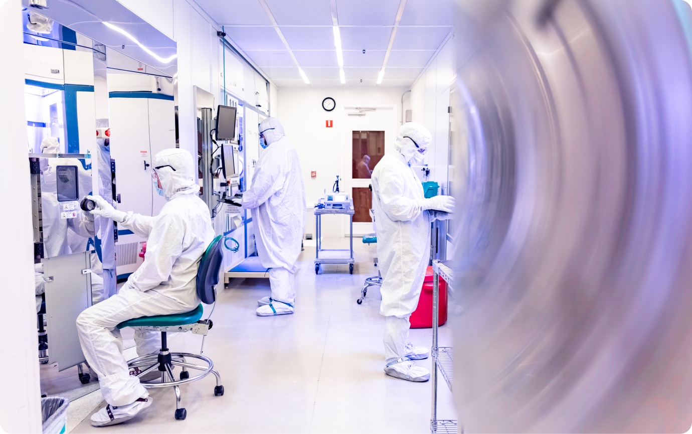
Atomica focuses on the success of our customers’ products, with rapid prototyping and scalable production. We are a leader in microfabrication, including photonics, sensors, biotechnology, and MEMS. We provide customers device optimization, faster speed to market, and cost-efficient fabrication. Atomica operates a 30,000-square-foot class 100 cleanroom near Santa Barbara, California, supporting a wide range of capabilities and materials with ISO 9001 certification and ITAR registration. We leverage sophisticated process control analytics, artificial intelligence inspection, advanced metrology, and proprietary fab operations systems to maximize efficiency.

Next Steps
Learn more about MEMS in our What are MEMS post
Talk to our engineering team about your MEMS design
See how we created the world’s most sophisticated MEMS device.