Atomica AI Photonic Integration Platform Brings Optics, Electronics, Memory and Packaging Together

PRESS RELEASE
Atomica Launches AI Photonic Integration Platform to Address the Integration Bottleneck in AI Infrastructure
SANTA BARBARA, CA, August 11, 2026 /PRNewswire-PRWeb/
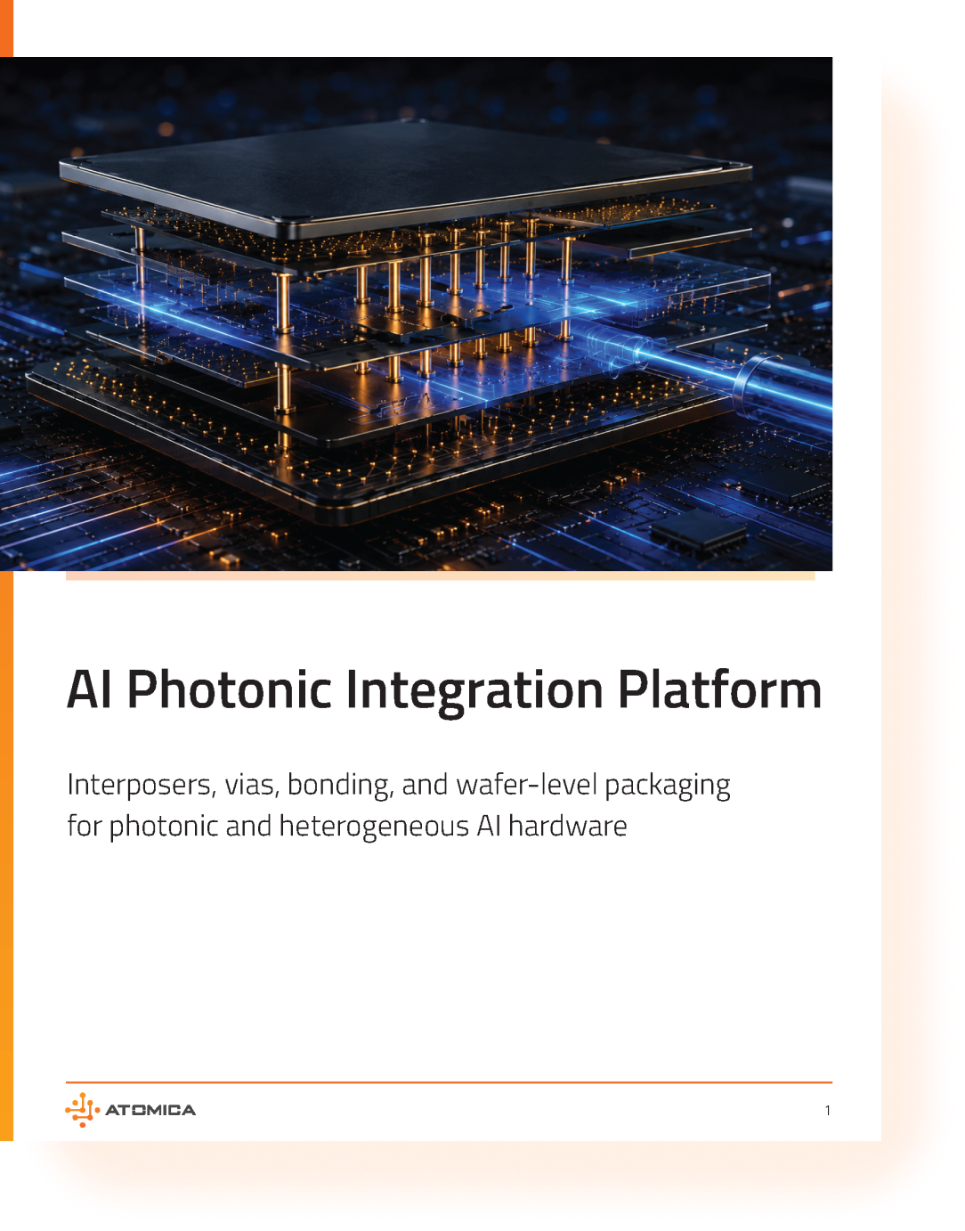
Atomica’s AI Photonic Integration Platform addresses a critical bottleneck in AI hardware: integrating optics, electronics, memory, thermal management, and packaging into one manufacturable system. The platform gives customers a configurable microfabrication pathway spanning interposers and vias, bonding, optical alignment, and wafer-level packaging.
Atomica, a U.S.-based microfabrication foundry, today announced the launch of its AI Photonic Integration Platform, a new microfabrication platform for customers developing photonic and heterogeneous AI hardware that integrates optics, electronics, memory, thermal structures, and package-level interfaces into compact, manufacturable systems.
The launch is the third in Atomica’s series of AI infrastructure platforms, following its AI Optical Connectivity Platform and AI Optical Source Platform. The three platforms address complementary parts of the AI optical hardware stack: moving and aligning light, generating and managing optical power, and integrating those optical functions with electronics, memory, routing, thermal management, and packaging.
AI hardware is increasingly constrained not only by processor performance, but by how effectively different devices can be connected and packaged together. As AI systems scale, bandwidth, interconnect density, signal integrity, thermal management, optical alignment, and package-level integration are becoming critical system challenges.
"AI hardware increasingly depends on integrating logic, memory, optics, and thermal management. Atomica's AI Photonic Integration Platform provides the microfabricated structures and manufacturing pathway to make that integration possible."

— Eldon Klaassen, CEO of Atomica
“The next leaps in AI hardware will not come from any single chip,” said Eldon Klaassen, CEO of Atomica. “They will come from integration — bringing logic, memory, optics, and thermal management together into a manufacturable system. That is where Atomica is focused.”
Atomica’s AI Photonic Integration Platform brings together microfabrication technologies for silicon and glass interposers, through-silicon and through-glass vias, redistribution layers, wafer-level packaging, bonding, cavities, optical alignment structures, and customer-specific process layers.
The platform is designed to support applications including AI accelerators, high-bandwidth memory integration, chiplet packages, data-center switches, optical I/O modules, co-packaged and near-packaged optics, photonic integrated circuit packaging, optical engines, external laser-source packages, advanced sensors, and physical-AI hardware.
At the center of the platform is heterogeneous integration. Photonic, electronic, memory, and thermal components may be fabricated on different substrates, use different materials, and have different alignment, stress, thermal, and reliability requirements. The challenge is bringing those elements together without compromising electrical performance, optical performance, or manufacturability.
“The challenge is no longer simply whether individual devices perform,” Klaassen said. “The challenge is whether optics, electronics, memory, and thermal structures can be integrated with the precision and repeatability required for scalable manufacturing.”
Rather than offering isolated process capabilities, Atomica’s platform provides a configurable development and manufacturing pathway. Customers can combine proven process modules with custom layers to support specific architectures and move from feasibility through prototype, manufacturing readiness, and scalable production.
The AI Photonic Integration Platform interfaces naturally with Atomica’s AI Optical Connectivity and AI Optical Source Platforms. Those platforms help generate, couple, align, and route light; the AI Photonic Integration Platform provides the substrate and package structures that integrate those optical functions with the rest of the system.
About Atomica
Atomica is a U.S.-based microfabrication foundry that builds advanced platforms for AI hardware, photonics, sensors, MEMS, and biotechnology devices.
Atomica delivers rapid prototyping and scalable production to customers developing AI optical connectivity, AI optical source integration, AI photonic integration, AI thermal microstructures, physical AI sensors, MEMS optical control systems, and biotechnology microdevices.
Atomica operates a 30,000-square-foot Class 100 cleanroom near Santa Barbara, California, supporting a wide range of capabilities and materials with ISO 9001 certification and ITAR registration. Capabilities include photolithography, deposition, dry etch, wet etch, bonding, plating, metrology, testing, dicing, and planarization.
Atomica leverages engineering collaboration, process standardization, modeling and simulation, AI-assisted optimization, and proprietary fab technology to achieve customer objectives.