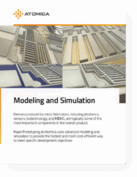
Atomica drives the success of our customers’ products with rapid prototyping and scalable production. Specializing in microfabrication for photonics, sensors, biotechnology, and MEMS, our ISO 9001-certified, ITAR-registered facility leverages advanced metrology, AI inspection, and proprietary process controls to deliver optimized, cost-efficient solutions.
Rapid Prototyping and Scalable Production
Atomica is dedicated to the success of our customers’ products, offering the fastest and most cost-efficient path to achieving development goals through Rapid Prototyping and Scalable Production. With state-of-the-art equipment, infrastructure, analytics, certifications, and quality assurance, we accelerate time to market while ensuring product excellence. While many fabs provide a range of tools and capabilities, Atomica stands out with its proven expertise in integrating complex layers and diverse materials, understanding their interactions, and delivering seamless, high-performance solutions. This experience is the key to helping our customers succeed in even the most demanding applications.
Specifically, we offer:
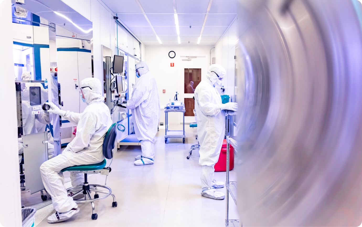
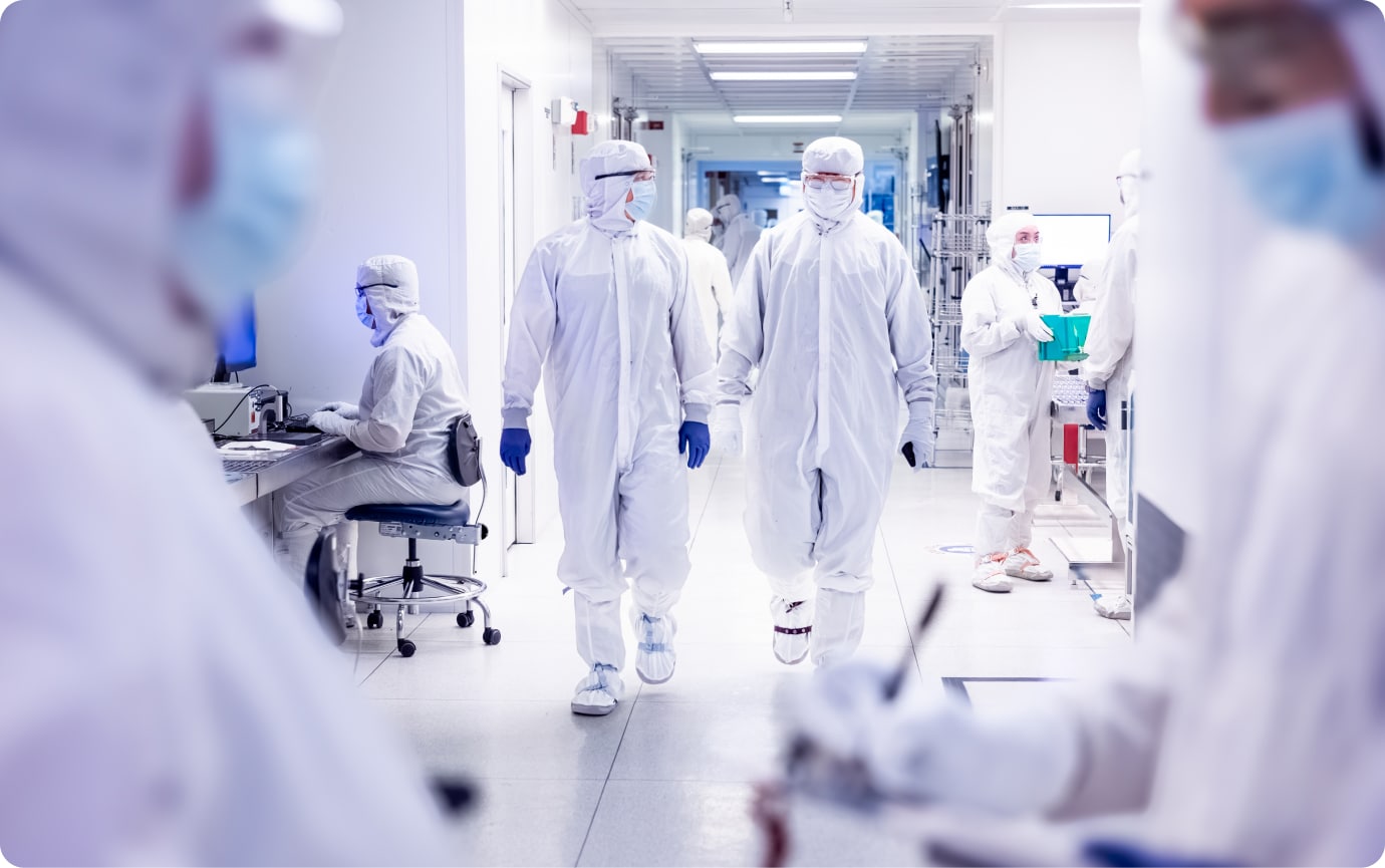
- 30,000-square-foot class 100 cleanroom fab for manufacturing 6″ and 8″ wafers
- Technical expertise in photonics, sensor, biotech and MEMS design, prototyping, and process development
- Complete analytical, metrology, and test capabilities for high-volume manufacturing with statistical quality control and statistical process control
- Volume foundry service for photonics, sensor, biotech and MEMS-specific or other wafer processing work
- Flexibility to develop and bring in new technologies
Capabilities
Design
Read about Atomica’s design and modeling services that complement our wafer foundry capabilities.
Lithography
Learn about Atomica’s photolithography technologies and leading-edge greyscale (3D) lithography.
Deposition
Discover Atomica’s deposition tools and its wide range of metals and dielectric deposition capabilities.
Plating
Discover how Atomica’s extensive range of plating tools and expertise unlock our unmatched material toolbox.
Annealing and Oxidation
Learn how Atomica’s Thermal Oxidation and Annealing processes play a crucial role in enhancing performance.
Dry Etching
Explore Atomica’s Deep Reactive Ion Etching (DRIE), Reactive Ion Etching and various other dry etch capabilities.
Wafer Bonding
Learn how Atomica’s bonding allows hermetic and vacuum wafer-level packaging.
Wafer Backend
Explore Atomica’s backend capabilities from CMP to wafer thinning to dicing.
Wafer Testing
Learn how Atomica’s in-process electrical, mechanical, and thermal testing enables real-time verification of functionality.
Metrology
Read how Atomica’s diverse metrology tools, enhanced with AI analysis, deliver precise, data-driven insights.
Explore Atomica’s in-depth resources to navigate modeling and simulation, rapid prototyping, scalable production, and fab evaluation — all with expert insight.
Why Atomica?
Atomica focuses on the success of our customers’ products, with rapid prototyping and scalable production. We are a leader in microfabrication, including photonics, sensors, biotechnology, and MEMS. We provide customers device optimization, faster speed to market, and cost-efficient fabrication. Atomica operates a 30,000-square-foot class 100 cleanroom near Santa Barbara, California, supporting a wide range of capabilities and materials with ISO 9001 certification and ITAR registration. We leverage sophisticated process control analytics, artificial intelligence inspection, advanced metrology, and proprietary fab operations systems to maximize efficiency.

