Applications
Thermal Imaging and Sensors
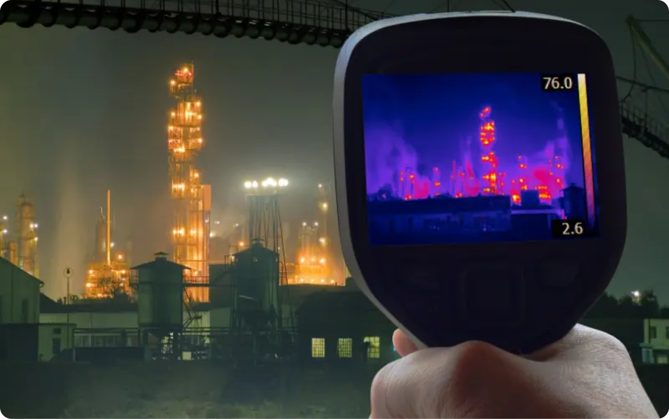
MEMS has transformed the thermal imaging industry with low-cost uncooled micro-bolometers and thermopiles for night vision, fever detection, and other thermal applications previously unavailable outside of the defense industry. These seemingly magical devices also empower humans to see in the long wave infrared (IR) spectrum (10-15 µm).
Atomica is pleased to help bring these innovations to life with our wafer processing, advanced DRIE, and getter deposition capabilities, particularly our proven vacuum wafer-level packaging (WLP) technologies.

Motion Sensors
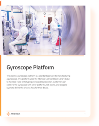
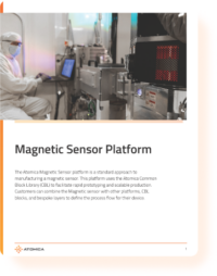
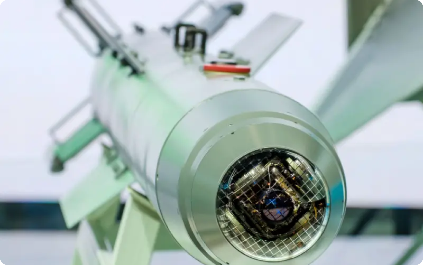
MEMS-based motion sensors are adding inertial intelligence to products across industries including automotive, consumer electronics, aerospace, healthcare, oil exploration, and more. MEMS wafer processing enables the fabrication of advanced accelerometers (for straight-line acceleration), gyroscopes (for rotation), magnetometers (for orientation), and collective inertial measurement units (IMUs).
Recognizing that off-the-shelf motion-sensing devices often do not provide the precision or performance required for specific applications, Atomica is proud to work with customers to fabricate custom motion sensors. Our world-leading DRIE, advanced photolithography, WLP, and other capabilities position us to tackle the most challenging projects in sensor development. We are even bringing optical sensors such as fiber optic gyros into the MEMS realm with the help of platform technologies like Atomica’s silicon optical bench (SiOB).
Microphones
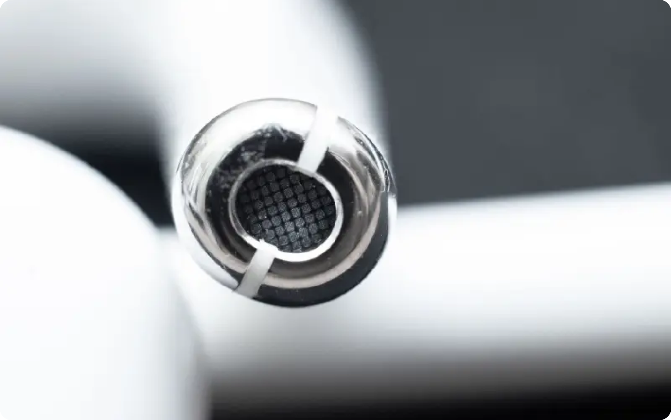
MEMS are driving the development of ever smaller, cheaper, and more sensitive microphones, in both analog and digital formats. Atomica’s mastery of complex wafer packaging using silicon and other advanced materials will help you bring cutting-edge acoustic sensing and response to your innovative device.

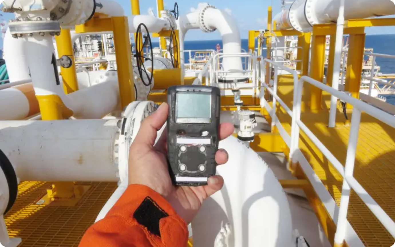
Gas and Chemical Sensors
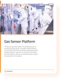
MEMS-based approaches to detecting gases and chemicals rely on electrochemical, pellistor, photoionization, and other advanced methods. MEMS-based gas and chemical sensors are smaller, more sensitive, and can have more functionality than traditional sensors, enabling exciting applications in industries such as defense, manufacturing, health, and energy.
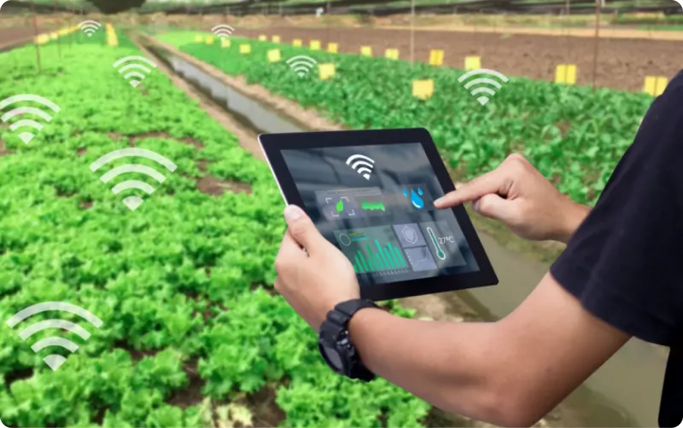
Other types of sensors:
Atomica offers experience and expertise in
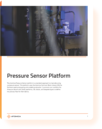
- Pressure sensors.
- Flow sensors
- Humidity sensors
- Magnetic / Hall effect sensors
- Radiation and x-ray sensors
- Radio frequency (RF) devices

Explore Atomica’s Sensor Platforms that enable rapid prototyping and scalable production of your device.
Why Atomica?
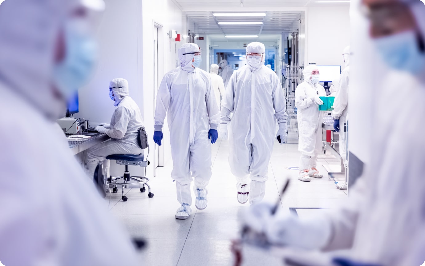
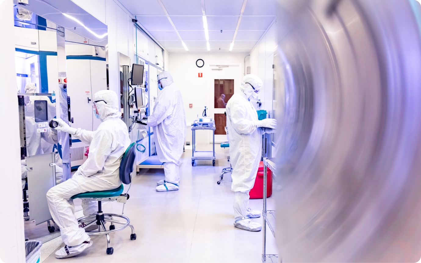
Atomica focuses on the success of our customers’ products, with rapid prototyping and scalable production. We are a leader in microfabrication, including photonics, sensors, biotechnology, and MEMS. We provide customers device optimization, faster speed to market, and cost-efficient fabrication. Atomica operates a 30,000-square-foot class 100 cleanroom near Santa Barbara, California, supporting a wide range of capabilities and materials with ISO 9001 certification and ITAR registration. We leverage sophisticated process control analytics, artificial intelligence inspection, advanced metrology, and proprietary fab operations systems to maximize efficiency.
