Atomica offers Cu via wafers as starting materials on 6” and 8” for standalone interposer applications:
- Wafers consist of back-filled plated Cu vias with top passivation layer
- Wafers are ready for custom redistribution layers, pad metals, and interlayer dielectric
Lead time:
6-10 weeks
(pending customization, quantity)
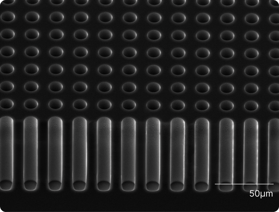
Via dimensions
Diameter:
<60µm
Minimum via pitch:
3x
diameter
Depth
<250µm
Via density per wafer
<5%
fill factor
Custom Post-Via Processing
Wafers are ready for customer’s specific design
Processes consist of the following:
- Top metallization, RDLs, and ILDs
- Backside polishing
- Backside passivation, metallization
Our Process Flow
01.
Via Etch

Via pattern, DRIE etch
Dielectric deposition
Dielectric deposition

02.
Cu Fill
Seed metal deposition
Electroplate Cu to fill vias
Electroplate Cu to fill vias
03.
CMP and Top Passivation
CMP Cu
Passivation deposition
Passivation deposition