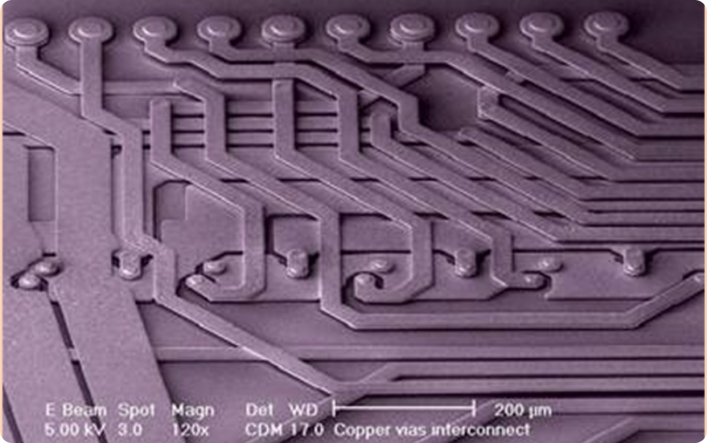
Atomica offers Through Silicon Via technology providing both standard and custom TSV interposer solutions, including electrochemically plated redistribution layers.
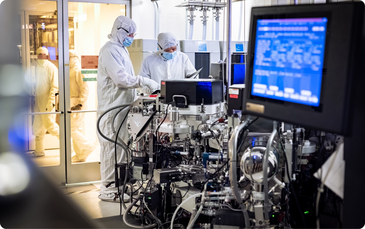
With cutting-edge tools and expertise in material science and bonding techniques, Atomica excels in creating high-quality TSVs, MEMS, and advanced 3D integrated packages.
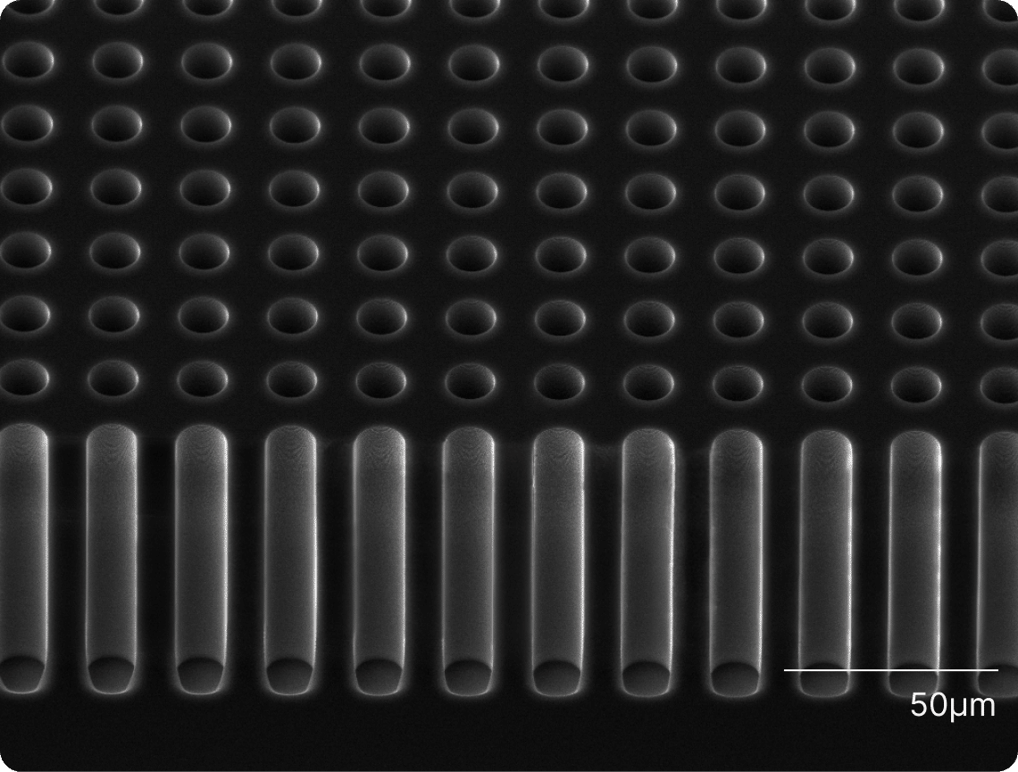
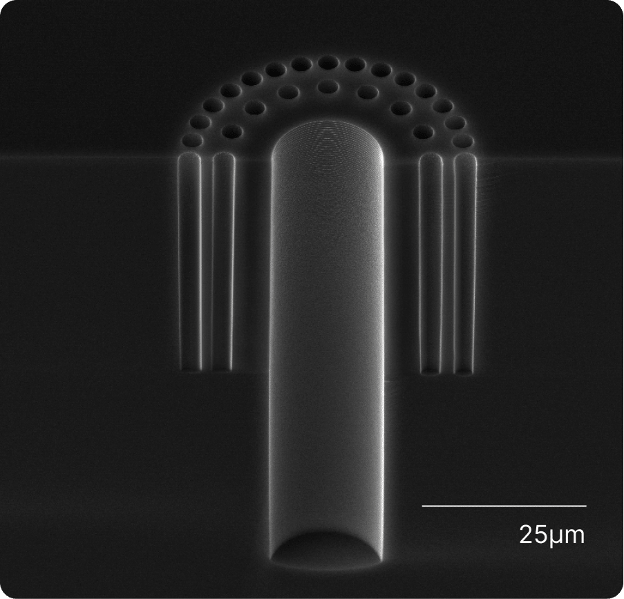
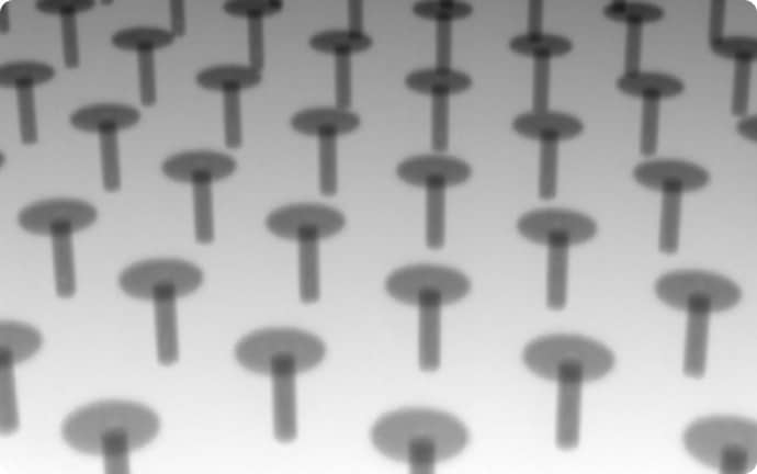
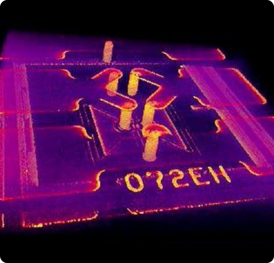
Through Silicon Vias (TSVs) are vertical electrical connections passing through silicon wafers or chips, enabling compact, multi-layer packages. TSVs allow smaller footprints, shorter signal paths, and increased integration. Through Silicon Vias are critical for 2.5D and 3D IC integrations, with future trends pointing towards heterogeneous 3D integration and the co-packaging of electronic circuits and MEMS. Through Silicon Via-enabled layers allow the combination of different materials and devices into a single package.
Get more in-depth with TSVs
Learn more about our customizable TSV Platform
Talk to our engineering team about your TSV project
Learn more about TSVs with our comprehensive guide
Extensive experience with Through silicon via technology
We meet diverse customer needs with both standard and customized Through Silicon Via solutions. Offering standard interposer platforms with TSV diameters ranging from 10 to 60 micrometers and a minimum pitch of twice the diameter, Atomica also excels in designing custom Through Silicon Vias with high aspect ratio and interposers tailored to specific requirements. This includes variations in silicon substrate thickness, TSV diameter, pitch, and aspect ratio.
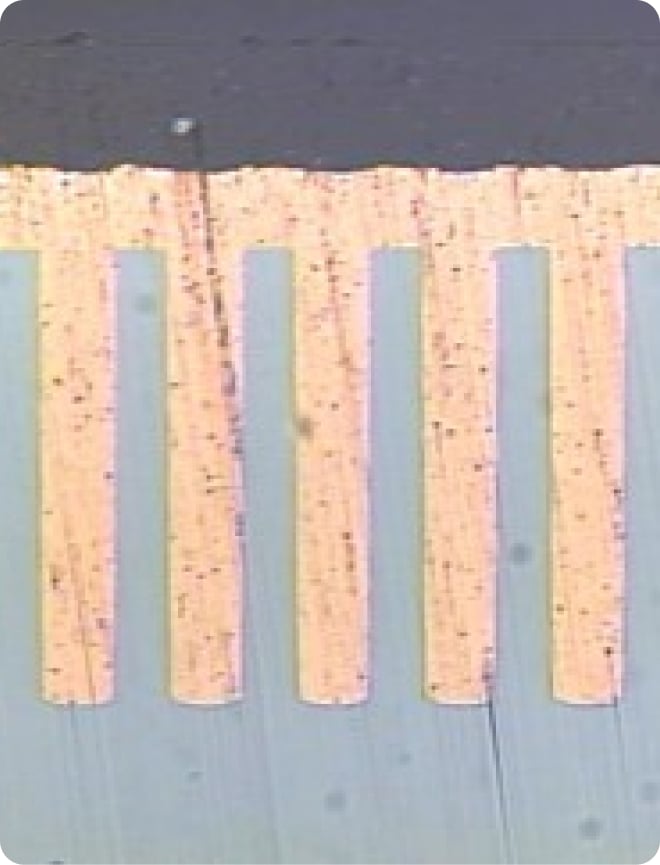
Atomica applies electrochemically plated redistribution layers (RDLs) on the interposer surfaces to form horizontal interconnects with the Through Silicon Vias, enhancing custom integration capabilities.
TSV Interposers:
MEMS Si interposers are enabling the next steps in efficiency of multi-layer 3D integration and wafer-level packaging, adding new functionality devices with electrical connectivity on extremely small footprint.
Why Atomica?
Atomica has the cutting-edge tools, sophisticated manufacturing processes, and expertise to create high-quality TSVs, MEMS, and advanced integrated packages. With deep experience in material science, Atomica offers a wide array of plating materials, including copper (Cu), gold (Au), silver (Ag), indium (In), nickel (Ni), tin (Sn), and alloys such as iron-nickel (NiFe) and gold-tin (AuSn). Atomica’s outstanding capabilities in bonding techniques, including thermal compression, fusion, direct bonding, polymer bonding, and hybrid bonding, enable unique solutions like bonding stacks of four silicon wafers (3D vertical 4 chips packages- Si cubes).

Next Steps
Learn more about our customizable TSV Platform.
Talk to our engineering team about your TSV project.
Learn more about TSVs with our comprehensive guide.