Photonics

Atomica helps bring innovative optical and photonic components to life.

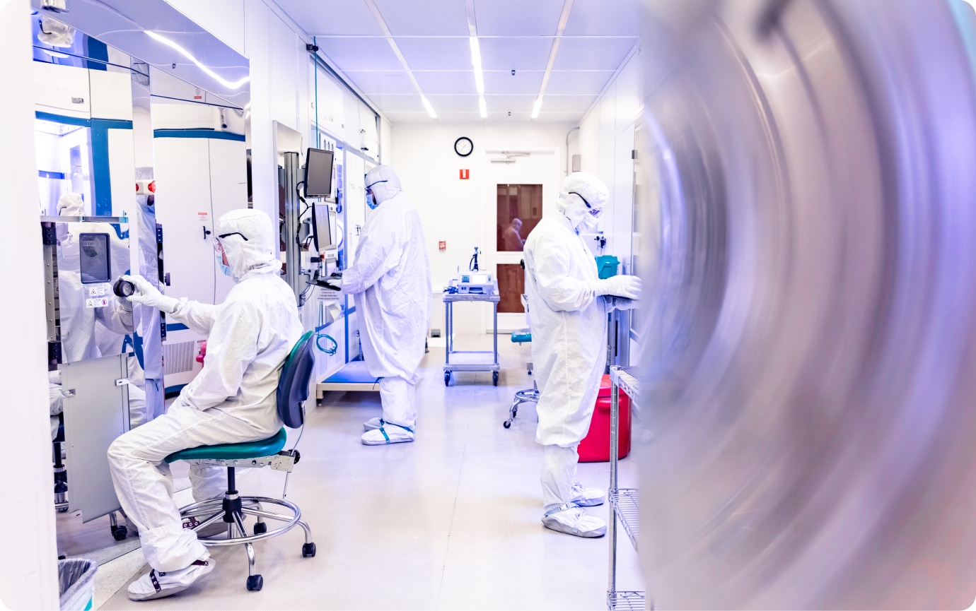
Our 20+ years of experience spans all manner of materials, structures, and applications, including optical communications, 3D sensing and LiDAR, augmented/virtual reality (AR/VR), thermal imaging, illumination, and other types of optical sensing.

Our customers in the photonics industry get a head start commercializing products by leveraging Atomica’s standard processes and platforms. Our people and processes can help you save money, establish a competitive advantage, and shorten time to market.

Applications

Optical Communications

As datacenters and telecom networks upgrade to 400 Gb and faster data rates, smaller and more precise micro-optical systems have become ever more critical. Atomica has broad and deep expertise in optical MEMS and wafer-level optical integration that enables higher levels of performance and integration. Below are some examples of our standard processes, platforms, and capabilities designed to advance photonic systems.

Explore Atomica’s Photonics Platforms that enable rapid prototyping and scalable production of your device.

interposer-platform

Interposer Platform

Understand how Atomica’s Interposer platform helps customers use standard structures for rapid prototyping and scalable production.

Get the Guide

microlens-platform

Microlens Platform

Gain insight into how Atomica’s Microlens platform allows customers to work with standard structures, enabling rapid prototyping and scalable manufacturing.

Get the Guide

micro-mirror

Micromirror Platform

Explore Atomica’s Micromirror platform, which lets customers utilize standardized structures to streamline prototyping and scalable manufacturing.

Get the Guide

siob-platform

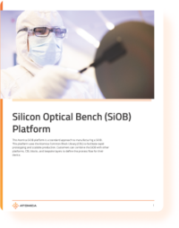
Silicon Optical Bench (SiOB) Platform

Learn more about how Atomica’s Microarray platform equips customers with standardized structures for rapid prototyping and scalable production.

Get the Guide

TGV-platform

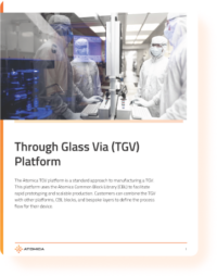
Through Glass Via (TGV) Platform

Examine how Atomica’s TGV platform gives customers access to standard structures, facilitating rapid prototyping and scalable production.

Get the Guide

tsv-platform

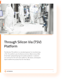
Through Silicon Via (TSV) Platform

Discover how Atomica’s TSV platform enables customers to leverage standard structures for rapid prototyping and scalable production.

Get the Guide

v-groove-platform

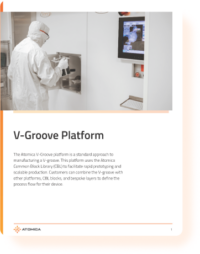
V Groove Platform

See how Atomica’s V Groove platform empowers customers by offering standard structures for rapid prototyping and production scalability.

Get the Guide

waveguide platform

Waveguide Platform

Uncover how Atomica’s Waveguide platform provides customers with access to standard structures, facilitating rapid prototyping and scalable production.

Get the Guide

wlp-platform

Wafer Level Packaging (WLP) Platform

Find out how Atomica’s WLP platform supports customers in leveraging standard structures to accelerate prototyping and expand production scalability.

Get the Guide

Why Atomica?

Atomica focuses on the success of our customers’ products, with rapid prototyping and scalable production. We are a leader in microfabrication, including photonics, sensors, biotechnology, and MEMS. We provide customers device optimization, faster speed to market, and cost-efficient fabrication. Atomica operates a 30,000-square-foot class 100 cleanroom near Santa Barbara, California, supporting a wide range of capabilities and materials with ISO 9001 certification and ITAR registration. We leverage sophisticated process control analytics, artificial intelligence inspection, advanced metrology, and proprietary fab operations systems to maximize efficiency.