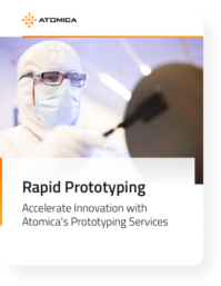
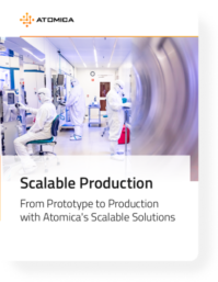
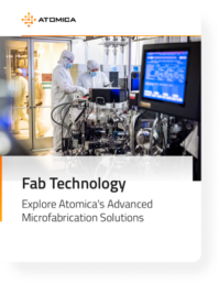
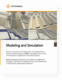
Atomica is a leader in microfabrication, including photonics, sensors, biotechnology, and MEMS. We focus on the success of our customers’ products, with rapid prototyping and scalable production. We provide customers device optimization, faster speed to market, and cost-efficient fabrication.
Our customers are manufacturers of advanced technology products for telecommunications, automotive, health care, aerospace and defense, industrial and consumer markets.
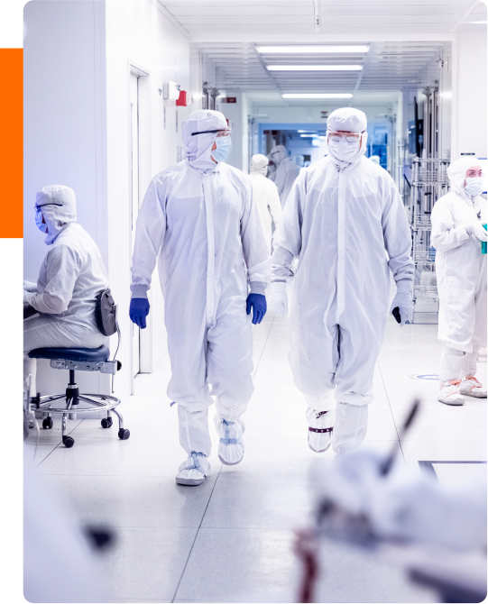
Atomica operates a 30,000 square foot class 100 cleanroom near Santa Barbara, California, supporting a wide range of capabilities and materials with ISO 9001 certification and ITAR registration. Atomica leverages sophisticated process control analytics, artificial intelligence inspection, advanced metrology, and proprietary fab operations systems to maximize efficiency.
Company Facilities
Atomica is one of the largest microfabrication foundries in the US, providing close collaboration for North American customers and the assurance that intellectual property is protected and respected. The company is privately held and controlled by Cerium Technology.
- 13-acre, 130,000 ft2 manufacturing facility with the capacity to support high-volume production
- 30,000 ft2 class 100 cleanroom
- Over 400 tools for both 6” and 8” wafer production
- ISO 9001 certified (since 2006)
- ITAR registered
- Broad materials flexibility, providing access to an extensive set of processes and materials unavailable in CMOS fabs, including noble metals, polymers, and virtually any substrate (e.g., silicon, SOI, glass, fused silica, quartz, borosilicate, piezos, and III-V).
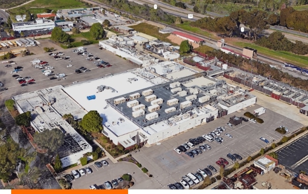
Atomica is located in the Santa Barbara area (Goleta, California) next door to the University of California, Santa Barbara, one of the top engineering universities in the world. This talent pool combines with Atomica’s multi-disciplinary team of scientists and manufacturing engineers to tackle the hardest process development and integration challenges with an eye toward manufacturability.


