Photonics platforms

Atomica’s photonics platforms use the Common Block Library (CBL), a set of standard, parameterized process blocks for rapid prototyping and scalable production. Platforms, CBL blocks and custom layers can be combined to define the process flow for a device.

01. OPTICAL ELEMENTS AND ALIGNMENT

Microlens Platform

Focus, collect and shape light in compact optical systems

Atomica’s Microlens Platform provides a foundation for individual lenses and arrays that focus, collect and shape light. Lens curvature, diameter and material determine focal length and optical behavior. Fabrication considers surface smoothness, refractive-index uniformity and alignment across an array. Lens geometry and coating choices are developed around the operating wavelength, with integration features that position each lens relative to adjacent components.

Micromirror Platform

Control beam direction with precise MEMS motion

The Micromirror Platform supports movable reflective surfaces that tilt or rotate to control the direction of light. Mirrors are suspended on torsion springs or flexible hinges, with actuation chosen for the required motion and control. Development addresses surface flatness, reflective coatings, electrode gaps and suspension geometry. Mirror size, deflection range and packaging are considered together to preserve optical quality and protect the moving elements.

Waveguide Platform

Guide light through photonic circuits and AR displays

Atomica’s Waveguide Platform supports optical routing on photonic chips and planar waveguides for augmented reality displays. Chip-based waveguides confine and route light between components, while display waveguides guide image light across a transparent substrate and direct it toward the eye. Materials, optical geometry and coupling features are matched to the operating wavelength and application. Fabrication controls dimensions, surface quality and pattern alignment to support efficient transmission, with packaging and thermal behavior evaluated to maintain optical performance.

V-Groove Platform

Position fibers for repeatable optical coupling

The V-Groove Platform provides alignment channels that locate optical fibers relative to one another and to nearby photonic components. In silicon, anisotropic etching uses the crystal orientation to define the groove profile. Groove width, depth and pitch determine fiber placement, while surface quality and array uniformity support consistent seating. These passive alignment features can be combined with optical benches and bonding steps in a complete device flow.

02. OPTICAL INTEGRATION AND PACKAGING

Silicon Optical Bench (SiOB) Platform

Align optical and electronic components on a shared substrate

Atomica’s Silicon Optical Bench Platform provides a silicon foundation for aligning and integrating lasers, lenses, detectors and other optical components. Etched mounting features, cavities and alignment marks establish component positions. Waveguides and electrical routing can be incorporated to connect elements across the bench. Development considers coupling accuracy, mechanical stability and heat dissipation, bringing optical and electronic interfaces together.

Interposer Platform

Connect multiple devices through a common routing layer

The Interposer Platform provides an intermediate substrate that connects photonic devices, electronics and package interfaces. Redistribution layers route signals across the surface, while through-wafer vias provide vertical connections where required. Substrate selection, routing pitch and layer alignment are developed around the electrical and mechanical requirements. Power distribution, signal integrity and thermal expansion are considered across the package.

Wafer Level Package (WLP) Platform

Protect devices with hermetic and vacuum packaging

Atomica’s Wafer Level Package Platform uses silicon, glass, quartz and metals to protect delicate structures before wafer singulation. Packages routinely achieve over 99% hermeticity, with sub-mTorr vacuum packaging for high-vacuum applications. Production experience includes four- and five-wafer stacks, with bonding and thermal stress evaluated to maintain performance. Through-silicon vias (TSVs), through-glass vias (TGVs) and optical access features support integration while preserving the protected environment.

03. THROUGH-WAFER INTERCONNECT

Through Silicon Via (TSV) Platform

Route signals vertically through silicon for compact integration

The Through Silicon Via Platform creates electrical paths through a silicon wafer or die. Etched vias receive insulating and barrier layers before conductive material is deposited, linking circuitry on opposite surfaces or between stacked components. Via diameter, depth and spacing influence resistance, capacitance and fabrication complexity. Development coordinates etching, metallization and wafer thinning while addressing thermal stress and interconnect reliability.

Through Glass Via (TGV) Platform

Combine vertical electrical routing with an insulating glass substrate

Atomica’s Through Glass Via Platform creates conductive paths through glass for vertical signal and power routing. Holes formed in the substrate are coated or filled with metal, connecting features on opposite surfaces. Glass provides electrical isolation and can preserve optical access around the vias. Development considers glass composition, via geometry, metal coverage and adhesion, with thermal expansion and mechanical stress evaluated for the integrated device.

Applications

Optical communications

Coupling and integration for transceivers, optical engines and optical switches

Datacenter and telecom networks need optical links that carry more data within tighter space and power budgets. Transceivers, optical engines and optical switches depend on accurate coupling and stable integration.

Atomica supports these systems with micro-optics, fiber alignment, optical benches and interconnect platforms, helping customers bring light sources, photonic devices and electronics into compact assemblies.

LiDAR and 3D sensing

Beam steering, light collection and alignment for depth-sensing systems

Depth measurements help vehicles and robots navigate, support biometric recognition and enable industrial inspection. LiDAR and other 3D sensing systems use controlled illumination and collected reflections to map their surroundings.

Atomica’s micromirror, microlens and optical bench platforms support beam steering, light collection and component alignment in compact optical assemblies developed around the sensing design.

AR and VR displays

Light shaping and scanning within the size and weight limits of a headset

AR and VR systems support training, design, entertainment and visual guidance by placing digital information in the user’s field of view. Compact optics must deliver clear images within the size and weight limits of a headset.

Atomica’s microlens and micromirror platforms support light shaping and scanning, with optical integration and packaging developed around the display architecture and its alignment requirements.

Medical and industrial imaging

Focusing, scanning and alignment for endoscopy, OCT and machine vision

Endoscopy, optical coherence tomography and machine vision bring detailed images to medical diagnostics and industrial inspection. These instruments need to direct illumination and collect light within compact optical paths.

Atomica supports focusing, scanning and component alignment through its microlens, micromirror and optical bench platforms, with fabrication tailored to the instrument’s geometry and optical requirements.

Quantum photonics and spectroscopy

Stable positioning and efficient coupling for sensitive measurements

Quantum photonics and spectroscopy depend on controlling light as it travels between sources, optical elements and detectors. Stable positioning and efficient coupling help preserve the signals these systems measure or manipulate.

Atomica’s optical benches, waveguides and alignment platforms provide a fabrication foundation for compact assemblies, with material and packaging choices evaluated around the optical design.

Building for AI infrastructure?

Explore AI Optical Connectivity, AI Optical Source and AI Photonic Integration for platform combinations tailored to AI optical links, laser integration and photonic packaging.

The same micromirrors, actuators, sensors, microfluidic channels and wafer-level packaging Atomica builds here power its five AI Infrastructure platforms: optical connectivity, optical sources, photonic integration, thermal microstructures and physical AI sensors, with a development path shaped for AI data centers and physical AI systems.

Explore the AI platforms →

Why Atomica?

A manufacturable path from prototype to production

Atomica is a U.S.-based microfabrication foundry that turns advanced device concepts into manufacturable, scalable hardware — and its advantage is not a single process but a system that de-risks the path from first prototype to volume.

30,000 sq ft cleanroom · Class 100 · ISO 9001 certified · ITAR registered · Santa Barbara, USA

1

Engineering Collaboration

Atomica works as an engineering partner across design, materials, fabrication, and testing, bringing diverse expertise together to optimize each micro-scale device. That collaboration is what yields better products, lower cost, faster time-to-market, and quicker adaptation to emerging technologies.

2

Process Standardization

Standardized processes give a clear framework for fabrication, scaling, and quality control. This is what delivers the consistency, quality, and efficiency that reliable, high-performance microdevices require — while supporting regulatory compliance and continuous improvement.

3

Modeling & Simulation

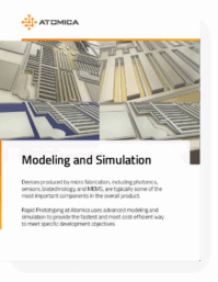
Atomica evaluates designs before fabrication using physics-based modeling, FEA, CFD, AI, and multiphysics simulation. Simulating first reduces prototype iterations, lowers cost, identifies risks early, and improves first-pass success across photonics, sensors, biotech devices, MEMS, and integrated microsystems.

4

AI Optimization (FabOps)

Atomica’s FabOps system applies AI and advanced analytics across wafer inspection, metrology, fab control, and project execution. By integrating equipment, process flows, pricing, projects, and manufacturing — with real-time visibility, lot tracking, and change control — it reduces risk and accelerates programs from prototype to scalable production.

5

Fab Technology

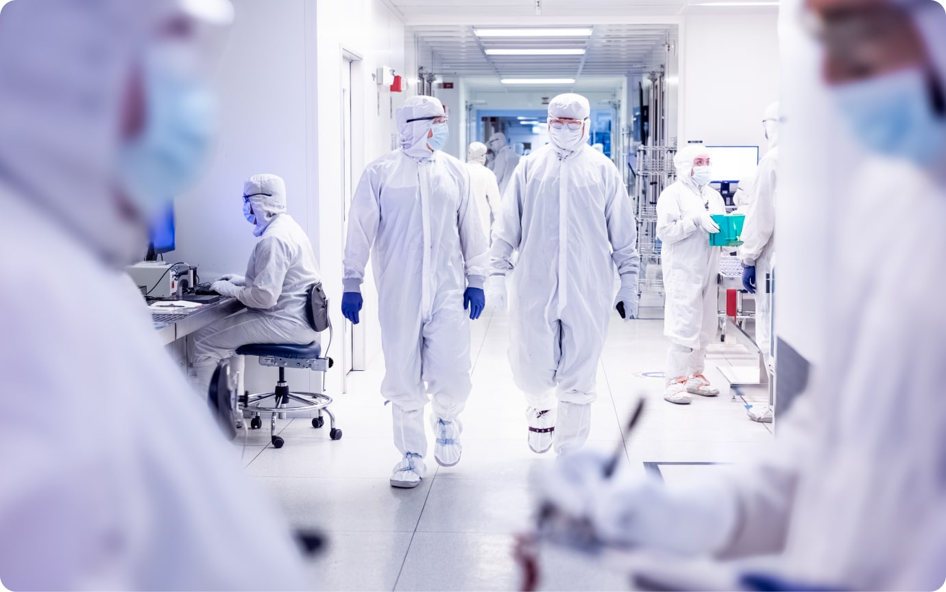
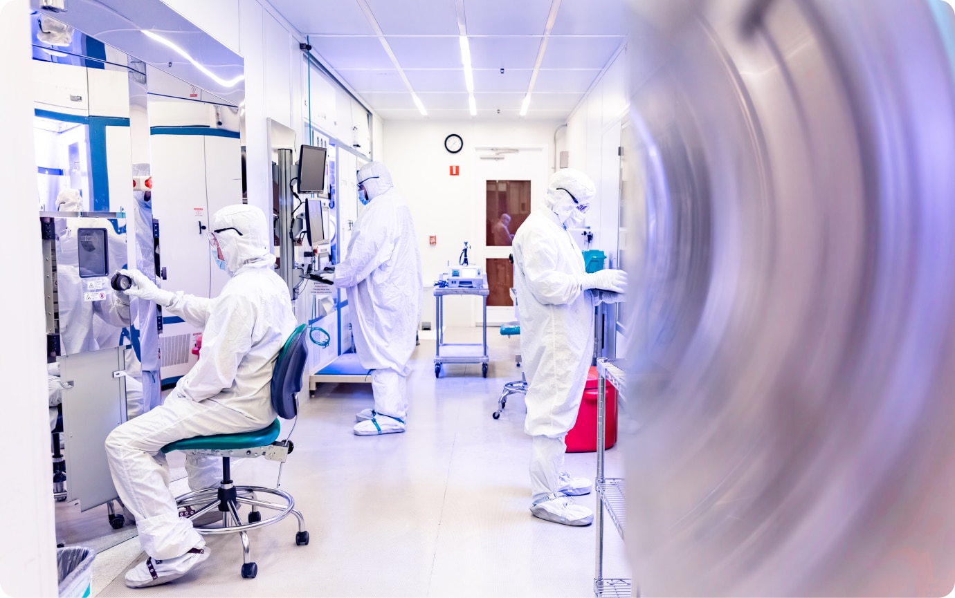
Atomica operates a 30,000 sq ft, class-100 cleanroom near Santa Barbara, California — ISO 9001 certified and ITAR registered. Its full in-house process suite spans photolithography, deposition, dry and wet etch, bonding, plating, metrology, testing, dicing, and planarization, purpose-built for rapid prototyping and scalable production.
Explore Atomica’s in-depth resources to navigate modeling and simulation, rapid prototyping, scalable production, and fab evaluation — all with expert insight.
Rapid Prototyping Services at Atomica

Uncover our efficient process that turns ideas into working prototypes swiftly, helping you bring innovations to life quickly.
Get the Guide

Scaling Production with Atomica’s Expertise

Explore how our advanced production methods ensure consistent, high-quality, and cost-effective results at every stage of scale.

Get the Guide

Inside Atomica’s Advanced Fab Technology

Take a detailed look at our high-tech capabilities, engineered to support complex, precision-driven microfabrication.

Get the Guide

Selecting the Right Fab for Your Project

Our Fab Evaluation Guide outlines essential criteria, ensuring your project is matched to the best fabrication partner.
Get the Guide

Simulation-Driven Microfabrication

See how modeling and simulation improve performance, lower cost, shorten timelines, and drive better outcomes.

Get the Guide

Next Steps

Building a photonic system? Talk to an Atomica engineer about the structures your device needs to move from prototype to volume.

Evaluating a microfabrication partner for photonics? Download our Fab Evaluation Guide to compare capabilities, processes, and scale-readiness before you commit.